Based on the self-developed “multi-channel high-power LED lighting centralized control system based on redundant technologyâ€, Maoshuo Power is listed in the 2011 National Key New Product Plan. The national key new product plan adopted this time is jointly named by the Ministry of Science and Technology, the Ministry of Commerce, the Ministry of Environmental Protection, and the General Administration of Quality Supervision, Inspection and Quarantine. The focus is on cultivating and developing national strategic emerging industries, with a focus on supporting independent intellectual property rights and technological content. High innovative products are designed to encourage enterprises to independently develop new products and promote the transformation and industrialization of scientific and technological achievements.
4 Layer PCB
Four-layer circuit board is a kind of Printed Circuit Board. It is made of four layers of glass fibre, which can reduce the cost of PCB.
There are also great differences between the 2-layer and 4-layer PCB. For details, please click: What's the difference between 2 layer and 4 layer PCBs?
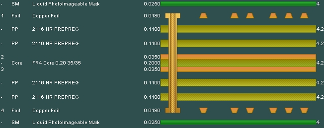
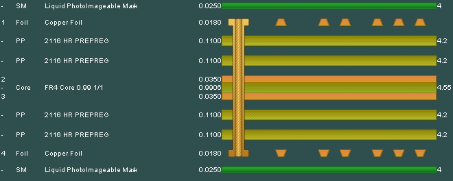
4 layer PCB stackup include two inner layers, inner layer 1 and 2, are sandwiched between the top and bottom layers. From top to bottom, the 4-layer PCB stackup like below ,The top, i.e. the signal layer (0.0014 in. width) is followed by a prepreg layer with a thickness of 0.0091 in. and dielectric constant of 4.2. The top layer is copper material. The prepreg layer is followed by inner layer 1 (0.0014 in.), referred to as the plane. A core sublayer is part of inner layer 1, which has a width of 0.037 in. This is followed by inner layer 2, which is another plane layer made with 1 oz. copper and is 0.0014 in. thick. Another prepreg sublayer constituting two sheets that are 0.0091 in. thick forms part of inner layer 2. The final layer, the bottom layer, is also 0.0014 in. thick, and is a signal layer as well. Interconnects are soldered and placed on the top and bottom layers.
The standard 4-layer PCB stack is shown below, and GND and VCC can be switched according to the layer with more signals.
If you don't want to connect all the ground pins through the hole, there will be different stacks and wide power routing on the signal plane.
4 LAYER 0.8 MM STANDARD BUILD
4 LAYER 1.6 MM STANDARD BUILD
0.4mm, 0.6mm, 0.8mm, 1.0mm, 1.2mm, 1.6mm, 2.0mm, 2.4mm, Please contact us if your board exceeds these.
Cost of four layer PCB is higher than double sided PCB because of complexity of design and higher sensitivity. The better quality of signals, achieved by reducing distortion and propagation levels, is also a factor. Because of the higher levels of signal integrity and reduced interference levels, more manufacturers prefer four layer PCB.
4 Layer PCB Printed Circuit Board,4 Layer PCB,4 Layer PCB Board,4 Layer Printed Circuit Board JingHongYi PCB (HK) Co., Limited , https://www.pcbjhy.com
When Maoshuo Power was first established in 2006, it set up a research and development center in Hangzhou and set up a research and development team of more than 100 people. It took 2 years to invest tens of millions of dollars and hired experienced international power supply design experts to lead the development of LED street lights. The tunnel light driving power supply officially launched the Maoshuo LED street light and tunnel light series driving power supply in March 2008.
From the beginning of the product launch, the sales volume and market share of Maoshuo Power increased. In 2010, Moso Power's market share of LED high-power street lamp driving power has exceeded half.
It is understood that Moso Power's products have never left the high reliability test since the beginning of design. The strict control and testing of the research institutes, pre-research departments and design departments provide effective protection for the products from the research and development of design solutions to the construction of the platform to providing supporting solutions for customers. Over the years, Moso Power has obtained more than 100 LED drive inventions, utility models, appearances and other patents, which has become a veritable industry standard "leader" for LED drive power.
Major projects unveiled to build well-known brands
At present, the seven-star series of products launched by Moso Power have passed CE certification. At the same time, Maoshuo Power has more than 2,000 customers worldwide, and has a wide range of applications in many key projects at home and abroad, such as the main venue of the 26th National Games, “Spring Festivalâ€, Shenzhen Jingji 100 Building, Xiangjiang First Tunnel, Guangzhou Lighting projects for a series of venues, roads and tunnels such as TV Tower, Yantai Binhai Square and Beijing-Zhuhai Expressway. The winning bids of many major projects at home and abroad have made Maoshuo Power not only famous, but also withstood the test of many market applications, which has created a golden sign for Maoshuo Power.
Grateful care lights the dreams of mountain children
At the end of 2011, Maoshuo Boai Primary School in Kuanping Township, Sinan County, Guizhou Province, which was funded by Maoshuo Power, was officially completed. For many years, Maoshuo Power has been committed to charity and has donated money and materials to disaster-affected areas such as the Wenchuan earthquake and the Yushu earthquake. As the “leader†in the LED industry, Moso Power has been contributing to economic development while actively promoting poverty alleviation and helping the development of education in poverty-stricken areas. 
What is 4 layer PCB?
Compared with Double Sided PCB , multi-layer PCB have many advantages. They can be designed more compactly. They can greatly improve noise resistance and make layout easier.
4 layer PCB stackup and thickness

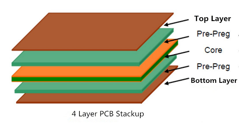
4-layer PCB has two stacking forms
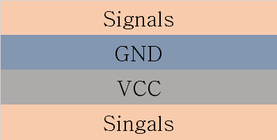
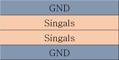
For the following reasons, this may be a better stack to use a four-layer PCB:
When the high-speed signal changes the reference plane, there should be a nearby path for its return current to move between the two reference planes. Using two horizons, you can do this by connecting two planes directly to a single channel. For grounding and power layers, the connection must be made through capacitors, which usually require two through-holes and one capacitor. This means worse signal integrity and more circuit board occupancy. On the other hand, having a power plane can reduce the voltage drop on the power rail, thereby releasing the space on the signal layer.
PCB Board Thickness
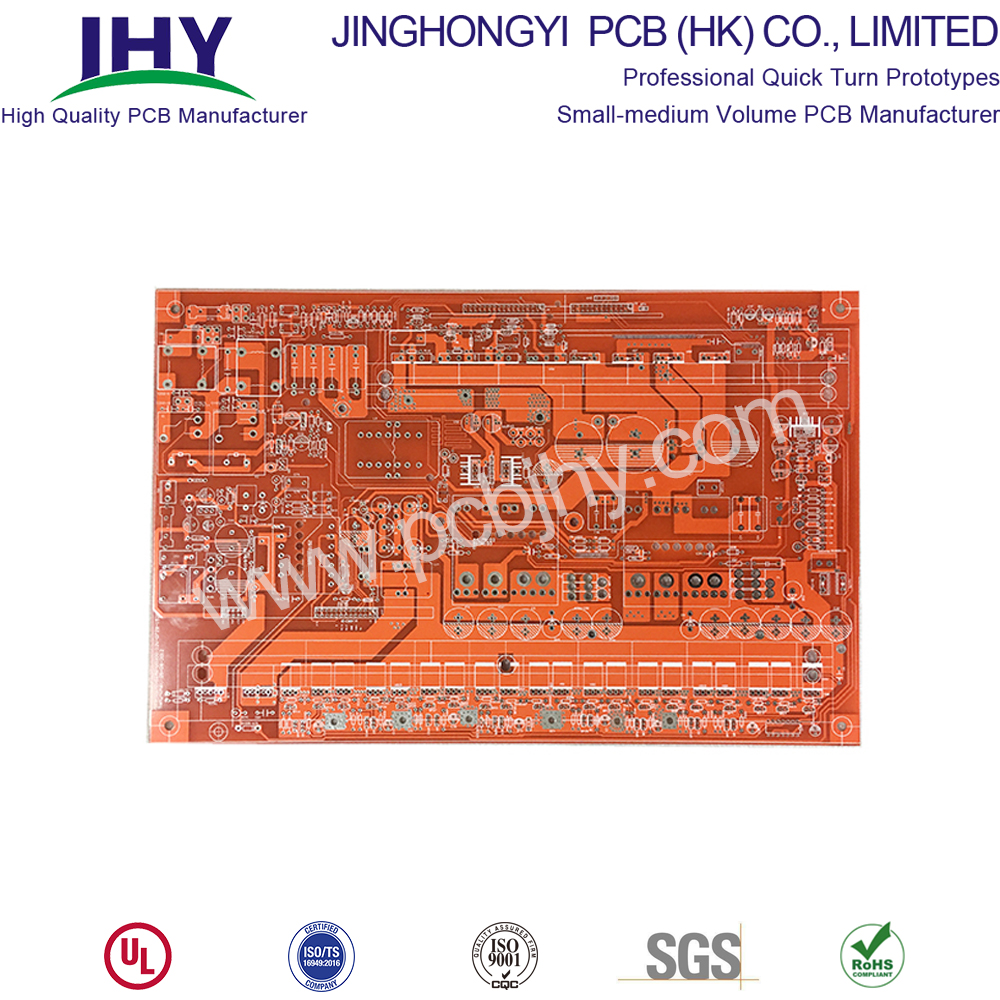
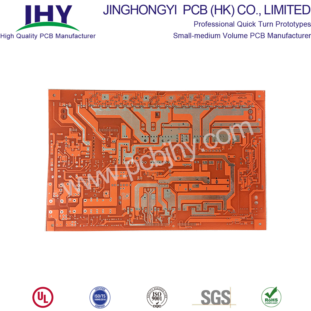
4 layer PCB Prototype
4-layer circuit board prototyping refers to the trial production of Printed Circuit Boards before mass production. It is mainly used for electronic engineers to design circuits and complete PCB Layout, then to carry out small-scale trial production process to the factory, that is, proofing PCB. The production quantity of four-ply proofing generally has no specific boundaries. Generally, engineers call it proofing before product design has not been confirmed and test has been completed.
Notices for proofing of four-layer circuit boards
The precautions for the production of four-layer PCB samples generally include two groups, one is the Engineer group, the other is the PCB Sample manufacturer.
As a group of engineers, the matters needing attention in proofing are as follows:
1. Choose proofing quantity carefully to control cost effectively.
2. Specially confirm device packaging to avoid proofing failure due to packaging errors.
3. Conduct comprehensive electrical inspection to improve the electrical performance of PCB board.
4. Make good signal integrity layout, reduce noise and improve PCB stability.
As a manufacturer of four-layer circuit boards, the precautions are as follows:
1. Check PCB files carefully to avoid data problems.
2. Conduct process approval in an all-round way and process configuration with self-manufacturer.
3. Control production quantity, reduce cost and maintain quality.
4. Communicate with customers who need samples to prevent accidents in advance.
4 layer PCB price and cost
We specialize in Quick Turn PCB services with an industry leading turnaround time as fast as 24 hours. Three low-cost options for a small number of PCB prototyping needs. At the same time, we also provided Flexible PCB , Rigid- Flex PCB , Metal Core PCB , High-TG PCB, Aluminum PCB , PCB Stencils, PCB Assembly Services and so on. Using the same high-tech equipment as our full-service PCB, it can be manufactured quickly and with virtually no limits.
4 layer PCB Manufacturing
We provide a full range of PCB functions to meet all your PCB needs. At present, we accept five PCB file formats (gerber file,.Pcb,.Pcbdoc.cam or.brd file format) for PCB manufacturing. But if you design a circuit board using Sprint-Layout software, you can send the. LAy6 file to us to manually generate the Gerber file.
JingHongyi PCB can provide you with multi-layer PCB board that meets RoHS standard. With laminated material, it can match high temperature in assembly process. It is important to remember that some lead-free assembly processes will require laminated substrates to withstand temperatures exceeding 260 degrees Celsius or 500 degrees Fahrenheit over a longer period of time. To solve this problem, we have high temperature laminates in stock, so that our customers can meet the higher temperature cycle requirements of some lead-free assembly applications.
Min. Order Quantity: 1 pcs
Material: FR-4
Finished Copper: 1oz/2oz/3oz(35μm/70μm/105μm)
Inner Layer Copper Thickness:1oz/1.5oz(35μm/50μm)
Silkscreen: White, Black, None
Surface Finishing: HASL with lead, HASL lead free, Immersion gold, Hard Gold ,OSP...
Shape: Custom Shape
100% Quality control
When making circuit boards, and after they are finished, we will test and inspect them strictly to ensure that the product reaches 100% eligibility rate. Preferential prices and higher quality have always been our constant pursuit:
Videos for 4 layer PCB design and manufacturing