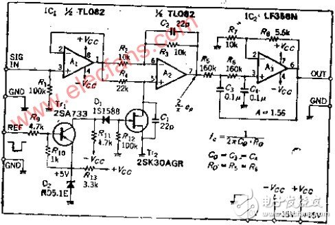
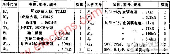
Circuit function The synchronous detection circuit with inverting and in-phase switching has an operating frequency of less than tens of kilohertz, and its DC stability must be applied to the double balanced differential circuit, which can be applied in the entire low frequency range. The analog switch of this circuit uses a general N-channel J-FET. The smoothing circuit adds a 12DB/OCT low-pass filter to reduce response time. The detection uses full-wave rectification, which makes it easy to eliminate higher harmonics. This circuit is widely used in lock-in amplifier detection circuits for measuring small voltages. The OP amplifier A1 is an impedance buffer. If the output impedance of the front stage is also low like the OP amplifier, A1 can be removed. A2 is an amplifier that performs inverting and non-inverting switching. TT2 is turned on, and the non-inverting input is grounded, and the amplification factor is -1 (-1=R3/R2). After the TT2 is turned off, the input signal is input to A2 via R4. Since the input resistance is very high, it becomes equipotential, and the inverting input must follow it, so TT2 acts as a follower with a magnification of 1. The analog switch circuit composed of TT2 must swing the gate-source voltage VOS in the negative direction to the pinch-off voltage VP. In order to drive with TTL level, +5/0V is replaced by -VCC/+5V, and it can also be replaced by CMOS analog switch, but the component cost must be considered. TT1 is a PNP transistor with an emitter voltage of -VCC. When the input TTL level is "L", TT1 generates the base current, TT1 is turned on, the collector electricity is placed near +5V, and the diode D1 is turned off, so ROS ≈ 0 and TT2 are turned on. Capacitors C1, C2 are added to reduce spikes. When the REF waveform that generates the reference phase is in phase with the input waveform, the output waveform of the OP amplifier A2 is a full-wave rectified wave of positive polarity, and the full-wave rectified wave of negative polarity when inverted, and the input waveform when there is a phase difference of 90 degrees. The polarity is converted at 90 degrees and 270 degrees to form s-shaped positive and negative symmetric waves. If smooth, the output is 0 regardless of the input signal size. If the peak value of the input voltage is set to E1, the average value of full-wave rectification is 2E1/π=0.636E1, and if the amplification factor of the filter is 1.56, a DC voltage substantially equal to E1 can be obtained at the output end. The composition of the low-pass filter adopts the same parameter method, and the cutoff frequency is determined by the output response, where FO takes 10HZ and the attenuation gradient is 12DB/OCT. In order to ensure accurate in-phase and reverse-phase conversion, R2=R3 must be made. The on-resistance TOE of TT2 should be equal to zero. However, there are actually several-surface ohmic resistors. It is possible to increase the resistance of R4 or the parallel resistance to reduce RON. The measures are resolved. The level switching circuit has a large number of components. For the sake of simplicity, VOB=0V, a cut-off N-channel MOS FET or a C-MOS analog switch can be used. Liquid Crystal Display For Instrument Liquid Crystal Display For Instrument,Large Industrial Precision Lcd Display,Small Industrial Body Thin Lcd Display,Precise Liquid Crystal Display Dongguan Yijia Optoelectronics Co., Ltd. , http://www.everbestlcdlcm.com