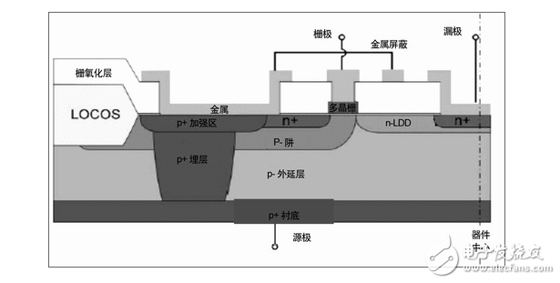
The largest application of RF power MOSFETs is the RF power amplifier in wireless communication. Until the mid-1990s, RF power MOSFETs also used silicon bipolar transistors or GaAs MOSFETs. By the late 1990s, the emergence of this situation changed. Compared with silicon bipolar transistors or GaAs MOSFETs, silicon-based LDMOSFETs have the advantages of low distortion, good linearity, and low cost, making them the mainstream technology of RF power MOSFETs. The output power of a power amplifier in a mobile phone base station ranges from 5W to over 250W. The RF power MOSFET is the most expensive component in a mobile phone base station. The cost of the RF portion of a typical cell phone base station is about $65,000, with the cost of the power amplifier reaching $40,000. Annual sales of power amplifier components are approximately $800 million. With the development of 3G, the demand for RF power amplifiers will be further improved. RF power MOSFETs are also used in the field of radio communications, and their frequencies have been extended to low microwave sections with output powers of more than 100 W. It is also used in television (especially digital TV) power amplifiers, radar systems and military communications. With the rapid development of new generation wireless communication technologies and the wider application, RF power MOSFETs have very optimistic market prospects. At present, RF power devices used in China still rely on imports, and domestic RF chips and devices have less than 1% of their own products. Therefore, it is very important to develop RF power MOSFETs independently. Figure 1 LDMOSFET basic structure Compared to silicon bipolar transistors, RF power LDMOSFETs have the following advantages: 1. Higher operating frequency and better stability: Bipolar transistors can only work in the frequency band below 300MHz, while LDMOSFET can work at frequencies from several hundred MHz to several GHz due to small feedback capacitance, and the frequency stability is good. 2. High gain: Usually at the same output power level, the gain of the bipolar transistor is 8dB~9dB, while the LDMOSFET can reach 14dB. 3. Good linearity and low distortion: Especially in digital signal transmission applications, LDMOSFET performance is more prominent. 4. Good thermal stability: temperature has negative feedback effect on LDMOSFET current, temperature rise can limit further increase of current; and bipolar transistor temperature has positive feedback effect on current, so LDMOSFET has good thermal stability. RF power LDMOSFET is a power MOSFET with a lateral channel structure. It uses LDMOSFET as the basic structure. It uses two diffusion techniques to successively perform boron and phosphorus diffusion in the same window, and precisely controls the groove by the difference of the depth of the two kinds of impurities. Road length. Its basic structure is shown in Figure 1, consisting of several key structures: 1. P+ substrate and P- epitaxial layer: The device generally uses a P+ silicon substrate plus a certain thickness of the P- epitaxial layer, and the P+ substrate is used for the source end to be well extracted from the back side; the P- epitaxial layer is for Increase the source-drain breakdown voltage of the device. 2. P-well, N+ source/drain, gate oxide, and poly gate: This is the basic element that makes up the MOS structure. P-well and N+ sources are formed by self-aligned implantation and double diffusion techniques. After the P-well and the N+ source are implanted, they are laterally diffused under the polycrystal, and finally the channel and source regions of the MOS are formed. 3. LDD structure: From the edge of the poly gate to the drain, it is a lightly doped LDD (Lightly Doped Drain) region, which can withstand the high voltage between source and drain. By optimizing the charge and length of the LDD region, the pass-through voltage of the source and drain can be maximized. In general, when the charge density of the LDD region is about 1011 cm-2 to 1013 cm-2, the maximum source-drain punch-through voltage can be obtained. 4. P+ buried layer: connect the surface source end and the P+ substrate. During operation, current flows from the source of the surface through the P+ buried layer to the P+ substrate and is taken out from the back side. This eliminates the need for additional leads from the front leads, reducing feedback capacitor inductance and improving frequency characteristics. 5. P+ enhancement zone (P+ enhancement) and metal shield (shield): The P+ enhancement zone is designed to ensure that current flows from the source end of the surface through the metal to the P+ buried layer. The metal shielding structure is to reduce the voltage of the poly gate by the edge of the LDD region and prevent the hot electron injection effect. By analyzing the performance and structural characteristics of RF power MOSFET devices, the basic structure of the device is designed and key parameters are obtained through process and device simulation. Key parameters of the device include: 1. Gate oxide thickness: The appropriate gate oxide thickness should be designed according to the threshold voltage of the device. 2. Channel length, impurity concentration and distribution: They determine the turn-on voltage of the device and the pass-through voltage between the source and drain must be specifically designed. 3. LDD length and impurity concentration: The LDD region shares the largest part of the source-drain voltage. Its length and impurity concentration distribution must be optimized so that the breakdown voltage of the device can reach a maximum value and the voltage distribution in the LDD region is uniform. 4. Epitaxial thickness and impurity concentration: they determine the longitudinal punch-through voltage between the N+ drain and the source from which the substrate is drawn. Combined with the 6-inch chip production line, the manufacturing process of the RF power MOSFET is completed, including: P+ buried layer, LOCOS, gate structure, P-well, source-drain and LDD structure, and contact hole, aluminum, and passivation layer. Process difficulties and solutions are as follows: 1. Gate structure: Special gate structure and process manufacturing process are designed to meet the function and frequency characteristics of the device. 2. Self-aligned implantation and double-diffusion processes in the P-well and N+ source regions: The device channel is formed by the lateral diffusion difference between boron and phosphorus during the P-well and N+ source regions. These two regions are formed by two polycrystalline single-sided self-aligned implants. The injection and propulsion processes need to be strictly controlled. 3. P+ well channel: The impurity concentration and length of this region are the key factors determining the performance of the device. The injection and propulsion processes must be strictly controlled in the manufacturing process to ensure the basic performance and uniformity of the device. By analyzing the performance and structural characteristics of RF power LDMOSFET, this paper designs the RF power LDMOSFET device structure, determines the key parameters through process and device simulation, and designs a set of manufacturing process flow conforming to the 6-inch chip production line, which is difficult in the process. Proposed a solution. Gold Finger Slot Connector,Dual Contact Gold Finger Slot Connector,High Current Slot Power Connector,Gold Finger Slot Power Connector Dongguan SOLEPIN Electronics Co., Ltd , https://www.wentae.com