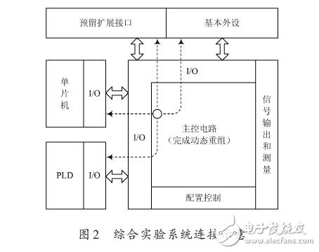
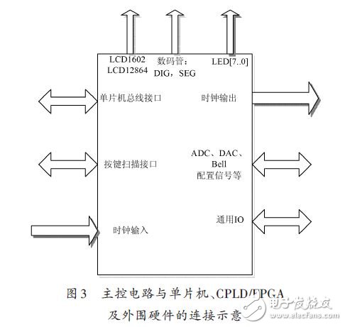
0 Preface “Digital Circuit and Logic Designâ€, “Programmable Logic Device and Applicationâ€, and “Single Chip Microcomputer Principle and Application†are important professional courses for electronic related majors. They occupy a very important position in electrical and electronic teaching and are also important for modern EDA technology. component. On the one hand, the three courses have strong practical application. The focus of student learning is to truly master the organic combination of hardware and software and the practical system application ability through practice. On the other hand, the three courses are closely related, and the “Digital Circuit and Logic Design†course is the foundation of the “Programmable Logic Device and Application†course. With the development of modern electronic technology, the traditional use of discrete components to complete digital circuit experiments. The method is also gradually replaced by programmable logic devices. At the same time, in practical engineering applications, it is often necessary to use 74 series devices and programmable logic devices to extend the peripheral circuits of the microcontroller. Therefore, the three courses are inseparable in the design of electronic systems. Although there are a variety of digital circuits, EDA or single-chip teaching equipment on the market, most of them are independent, "single-board" design patterns. Even if there are a small number of comprehensive experimental platforms, they are simply a few. The experimental resources of the course are integrated into an experimental platform, and then wire connections are used as needed, and there is no essential difference between the experimental platforms and the independent experimental platforms. In addition, the hardware circuits of some functional modules in different experimental platforms are the same; but on different experimental devices, the same modules cannot be shared, and there is a waste of resources. Finally, the integrated design is difficult to expand the function, which is not conducive to students' design of innovative projects. Under this circumstance, from the perspective of cultivating students' innovative spirit and improving the ability to comprehensively utilize the knowledge learned to solve practical problems in engineering, there is an urgent need for an experiment that can complete independent experiments for each course and complete comprehensive design experiments. platform. In order to solve the above problems, the experimental system adopts the method of circuit dynamic recombination to provide 8 modes from 0 to 7. In a set of experimental systems, it not only contains the functions of the common logic chip of digital circuit, but also the hardware resources of programmable logic device and single chip microcomputer. Can meet the teaching needs of the three courses at the same time. The experimental system also reserves an expansion interface, which can connect the designed extension circuit to the experimental system, which is beneficial to train students' innovative ability. 1 Comprehensive experimental system design The comprehensive experimental system adopts a design scheme in which the circuit can be dynamically reorganized, and its system structure block diagram is shown in FIG. 1 . The system is divided into: main control circuit module, single chip module, PLD module, human-computer interaction module, display module, matrix button module and reserved expansion interface module. The main control circuit module is the core of the dynamic configuration of the circuit, and can realize any connection between all resources. The human-computer interaction module provides a friendly configuration interface through the LCD12864 display and buttons, enabling mode selection, setting signal parameters, and observing measurement results. The display module and the matrix button module are collectively referred to as basic peripheral modules, and provide basic input and output resources. The integrated experimental system is also equipped with signal generation and detection functions to generate a square wave signal with adjustable frequency and to measure the frequency and voltage of the input signal. 1.1 main control circuit module The main control circuit module uses Altera's MAX II series EPM570T144C5N as the control chip. The MAXII series devices not only have the architecture and performance of the FPGA look-up table, but also have the functions of CPLD storage data non-volatile, easy to program and instantaneously turn on. The application is more flexible and convenient. This series of devices is not easy to identify by the user when programming, so it is classified into CPLD by Altera Company. The main control circuit realizes the dynamic reorganization of the circuit, which can be configured into different connections as needed. The different modes of the integrated experimental system, the connection is shown in Figure 2. The MCU module, PLD module, reserved expansion interface module, basic peripheral module, etc. are directly connected to the CPLD device EPM570T144C5N in the main control circuit through the standard I/O port (shown by the solid line double arrow). Because of the rich interconnects inside the device, data can be forwarded between different I/O interfaces by simple hardware programming, that is, the function of on-chip data routing is realized. Therefore, by programming the CPLD through the hardware description language HDL (Hardware DescripTIon Language), data forwarding between other functional modules can be completed, and an indirect connection between these modules is realized (shown by the open double arrow). For the user, the user only needs to perform configuration control through the human-computer interaction module, select the required mode, and can call the pre-stored different connection configuration information to automatically realize the dynamic connection between different modules of the experimental system. Specifically, there are three forms of connectivity: (1) Connect the basic peripheral module, reserved expansion interface module, signal generation and measurement to the PLD module to realize the function of the independent programmable logic device experimental platform. At the same time, the programmable logic device can also simulate the 74 series digital chip to realize the functions of the independent digital circuit and logic design experimental platform. (2) Connect the basic peripheral module, the reserved expansion interface module, the signal generation and measurement to the single-chip microcomputer module, and realize the function of the independent single-chip experimental platform. (3) Connect the MCU module to the PLD module, and then connect the basic peripheral module and the reserved expansion interface module through the PLD module to realize the function of the comprehensive experimental platform. For the user, these modules are directly connected, and the user can only access the various functional modules based on the dynamic recombination circuit. The specific connection circuit of the main control circuit EPM570T144C5 is shown in Figure 3. 1.2 MCU module The MCU module currently selects the device as SST89E516RD, which is an 8-bit MCU based on 8051 core produced by SST. The biggest feature is online download and online debugging. Its pin is compatible with AT89C51, clock frequency is 0~40 MHz, integrated with 1 KB of on-chip RAM, 64 KB+8 KB of FLASH E2PROM. In addition, the MCU module is also equipped with temperature sensor DS18B20, 8 KB serial E2PROMAT24C08. The plug-in is connected to the EPM570T144C5N and can be replaced as needed. 1.3 PLD Module This module can be replaced with different EDA core boards as needed. This experimental system uses a self-designed EDA core board, using Altera's Cyclone III series EP3C10E144C8, containing 10 320 logic units (LE), 46 M9K modules, 423Mbit RAM, and 23 18 & TImes; 18 hardware multipliers, 2 PLL, 10 Gclks. The EDA core board also provides 8 independent buttons, a 40 MHz active crystal. 1.4 Other peripheral hardware resources The human-computer interaction module, display module, and matrix button module also provide some common hardware resources, including: 10-bit high-precision A/D converter ADS7822, 12-bit high-precision D/A converter TLC5615, 8 LEDs, 8 common Yin 7-segment digital tube, character LCD 1602, dot matrix dot matrix LCD 12864, buzzer, 4 & TImes; 4 matrix buttons. 1.5 extended interface It can connect with other circuits through two 40-pin dual-row sockets of P3 and P4, and flexibly support various design projects, which is conducive to the training of students' comprehensive and innovative ability. Figure 4 shows the connection between the expansion interface and the core circuit EPM570T144C5N. 2 experimental system mode The integrated experimental system adopts a modular structure, and there are 8 modes from 0 to 7, which can be selected through the buttons S0~S4 in the human-computer interaction module. Modes 0~4 are microcontroller modes, and modes 5~7 are programmable logic device modes. In different modes, the structure of the circuit and the peripheral hardware resources are different. Shenzhen Scodeno Technology Co.,Ltd , https://www.scodenonet.com