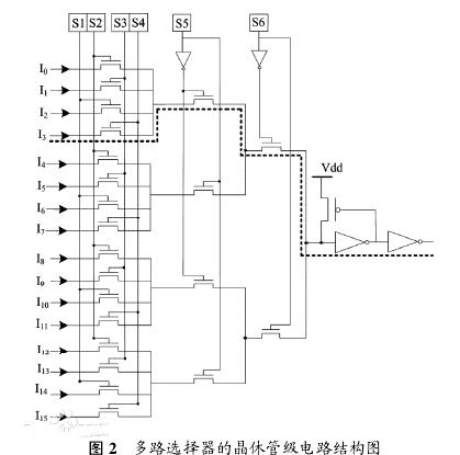
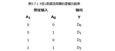
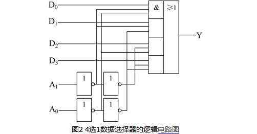
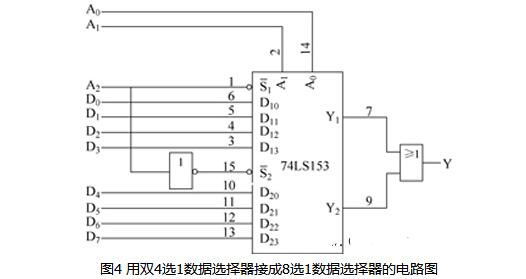
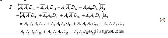
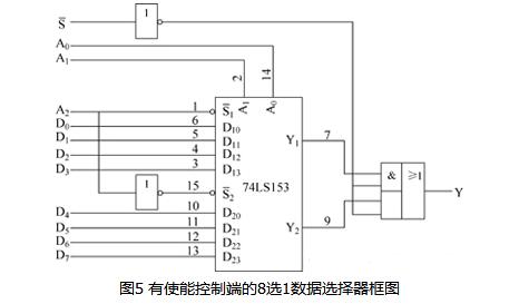
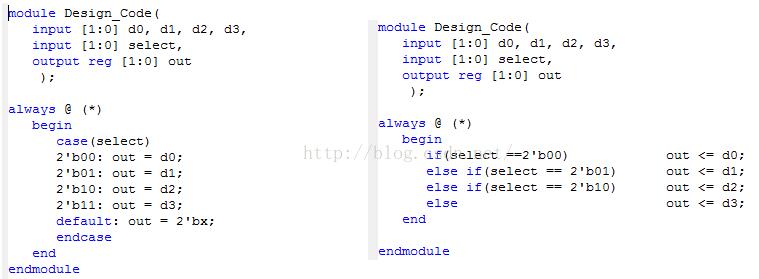
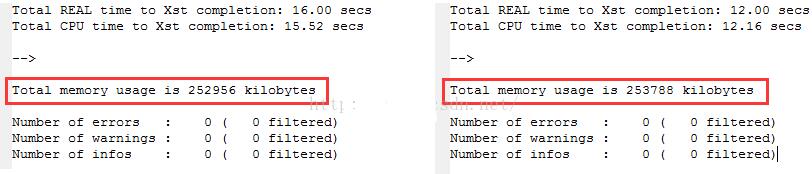
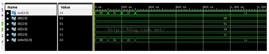
The multiplexer is an alias for the data selector. In the multi-channel data transmission process, a circuit capable of selecting any one of them according to need is called a data selector, which is also called a multiplexer or a multi-way switch. A typical FPGA device consists of three basic types of resources: configurable logic blocks (CLBs), routing resources, and programmable input/output modules. The programmable logic blocks are surrounded by prefabricated routing resource channels. Programmable input/output modules are distributed around the FPGA. In addition to the above three types of resources, the FPGA usually includes optional resources such as block RAM and multipliers. In various FPGA resources, the programmable logic block is a basic unit for implementing user functions. Each programmable logic block includes one interconnect switch matrix and four SLICEs. Each SLICE includes two lookup tables (Look-Up). -Table, LUT), 2 flip-flops, and some multiplexers. The interconnection switch matrix is ​​mainly composed of wires of different lengths and a plurality of wiring switches. A typical wiring switch structure is shown in FIG. 1 . As can be seen from Figure 1, each routing switch consists of a multiplexer, a buffer, and some programmable SRAM cells. Among them, the multiplex selector is a bridge that connects each routing track and programmable logic block. Its structure has a great influence on the performance and power consumption of the FPGA. Depending on the length of the wire driven by the multiplexer, the size of the multiplexer in the FPGA varies from 4 to 1 to 30 to 1. Figure 2 shows a 16-to-1 multiplexer-type transistor-level circuit configuration. The left side of the multiplexer is 16 input lines, which are used to connect resources such as routing tracks or programmable logic blocks. S1~S6 represent 6 programmable SRAM cells. You can select from 16 input lines by configuring the contents of the SRAM cells. One is used as a valid input. For example, when the storage value of the S1~S6 memory cells is “000100â€, the input line I3 is selected, and the effective path through which the signal passes is shown by the dotted line in FIG. 2 . The main part of the multiplexer is a transfer transistor. Since the carrier transfer efficiency of the NMOS transistor is high and the circuit speed is fast, the transfer transistors in the multiplexer are all implemented using NMOS transistors. The commonly used multi-way selector has four types of selection 1, 8, 1 and 16 selection 1 and the like. The following describes the working principle of the data selector with 4 selections and 1 data selector as an example. According to the functions of the data selector described above, the logic function table of 4 selection 1 data selectors can be listed, as shown in Table 5-7-1. Which D0 ~ D3 for the data input, A0, A1 for the data selection. The expression between the output and the input can be written by the logic function table as Draw a logical selection of 4 select 1 data selector logic 2 as shown. The 74LS153 is an integrated dual 4-select 1 data selector logic device. Figure 3 shows the logic diagram and block diagram of the 74LS153. As can be seen from Figure 3(a), the logic circuit of the 74LS153 includes two 4x1 data selectors whose data input ends are D10, D11, D12, D13 and D20, D21, D22, and D23, respectively, and the data output ends are respectively Y1 and Y2. They have common address selection inputs A0, A1. In addition, each has an enable control It can be seen from equation (2) that only when the control terminal is enabled The logic function table of 74LS153 is shown in Table 2. Table 2 Logical function table of 74LS153 Multiple data input multiplexers can be designed with multiple data input data selectors. Example 1: Design an 8-to-1 data selector with 74LS153. Solution: The 74LS153 is a dual 4 select 1 multiplexer. There are two common address selection inputs, eight data inputs. 8 Select 1 The data selector requires three address inputs (23 = 8), so the lack of an address input is required with the enable control. The circuit of the 8-to-1 data selector designed with a double 4-select 1 data selector chip 74LS153 is shown in FIG. 4 . When A2 = 0, the upper side of the 4 selection 1 data selector work, according to the state of the address input terminal A0, A1, the output terminal Y1 selects output D0 ~ D3, this time Y2 = 0, so Y = Y1; when A2 = 1 In this case, the lower 4 bits of the 1 data selector work. According to the state of the address input terminals A0 and A1, the output terminal Y2 selects and outputs D4 to D7. At this time, Y1=0, so Y=Y2. The logical function is You can also add an enable control to control the working status of the connected 8-to-1 data selector. The circuit for adding the 8-to-1 data selector of the enable control terminal is shown in FIG. As can be seen from FIG. 5, when =0, the 8-to-1 data selector operates normally; when =1, the output of the 8-to-1 data selector is locked at the low level. It can be seen from Table 2 that a 4-to-1 data selector with two address inputs A0, A1, when the enable control terminal = 0, the logical relationship between the output and the input is If A0 and A1 are used as two input variables, and D0 to D3 are the appropriate states of the third variable (including the original variable, the inverse variable, 0 and 1), you can use the 4-to-1 data selector to realize any form of Three variable combinational logic function. Similarly, a combinational logic function with any number of variables not greater than n+1 can be implemented with a multiplexer of n-bit address inputs. Example 2: Using the 4 Select 1 Data Selector to implement the following combinational logic function: Solution: Turn equation (4) into the form corresponding to equation (5): Comparing Equation (6) with Equation (4), we can see that the data input of the data selector is The output of the multiplexer is the combinatorial logic function to be expressed. Design a two-digit 4-way selector, because the selector uses the condition trigger method to match output and input to the truth table, so it can be associated with the conditional statements “If†and “Case†in the C program design. What are the differences between these two designs from the hardware point of view? code show as below: In order to distinguish between the two designs, you can view the comprehensive report provided by ISE, as follows: Comprehensive report comparison: Using Case Condition Statements Using IF Condition Statements From the comprehensive report, we can see that the if statement uses more components than the case statement uses. At the same time, each branch in the if statement has a priority (serial) and a similar cascade structure; the case statement is Branches are at the same priority (in parallel) and synthesis can result in a multiplexer. Therefore, for designing a multiplexer, the delay caused by the if statement is often larger than that of the case statement, so using a case statement will be better for the multiplexer. Latches may occur under the Case statement. A row of the case block under the comment case condition can get a 2-bit four-way selector under the incomplete case statement. It is known from the 2-bit four-way selector in the incomplete case statement that since all branches of the case statement are at the same priority, when the condition is not complete, it does not depend on the order of the statements, but only on the pending order. The signal, and the processing result is the processing result of the signal that is different from the signal to be processed by 1'b1. In this condition, the processing result corresponding to the signal having a difference of 1'b1 from the signal to be processed is latched and the latch is thus generated. . For latches and latches, the latch may latch on Glitch in the presence of Glitch in the pending signal, resulting in a serious latch error. This is a significant deviation from the intended signal processing result. Therefore, there is a destabilizing factor in the latch, so when using a latch, it is important to keep in mind that the Glitch of the signal to be processed is prioritized. Test file: Initial begin // Initialize Inputs D0 = 0; D1 = 1; D2 = 2; D3 = 3; Select = 0; #100; Select = 1; #100; Select = 2; #100; Select = 3; #100; // Add here End Simulation results:
This 80 -port USB charger: This 80 port USB charging station can quickly synchronize 80 devices to charge. This USB charging station multi -terminal charger can meet the needs of multiple people. Safe multi -end mouth charger center: This high -power fast charger has a solid aluminum metal frame to make the product long -term durable, built -in intelligent multiple security protection, can be used for over current, overvoltage, short circuit, etc. Hospital, ETC, etc.
80 Port Usb Charger,80 Port Mobile Charger,Multiple Usb Charging Station,Multi Port USB Charger shenzhen ns-idae technology co.,ltd , https://www.szbestchargers.com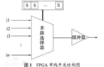

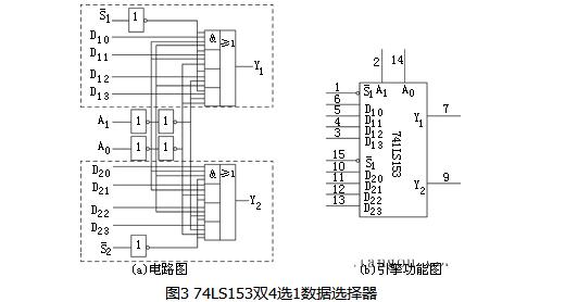
 . From Figure 3 (a) can be written between the input and output logic function is
 The data selector can work normally, otherwise the data output is locked at low level. Therefore, the enable control terminal is active low.
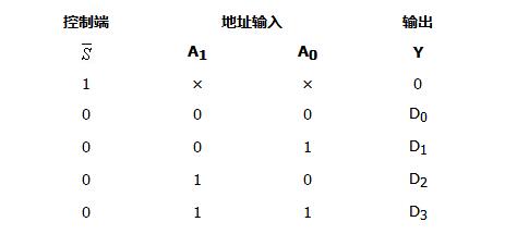


What is a multiplexer
80 Port USb Charging