Application of C5402 DMA combined with MCBSP in data acquisition system
1 Introduction
In a data acquisition system with C5402 DSP as the core, users generally need to process a piece of data after it has been collected. Collecting data by query method will consume a lot of CPU resources. Using interrupt mode to collect data can improve the CPU utilization, but it is still completed by the CPU at each moment of data acquisition, and the readability of the program is reduced. The data acquisition system designed in this paper uses C5402 memory direct storage control DMA and multi-channel buffer serial port McBSP to design the system, so that the normal operation of the CPU and DMA data acquisition in parallel, improve the operating efficiency of the DSP.
2. Features of C5402 DMA C5402 memory direct storage control DMA can realize the free transfer of data between DSP memories without occupying CPU resources. The C5402 has six independently programmable DMA channels, each of which is controlled by its own five 16-bit registers: source address register DMSRC, destination address register DMDST, unit count register DMCTR, synchronization event and frame count register DMSFC, transmit mode Control register DMMCR.
1. The source address register DMSRC specifies the first address of the source data to be transferred by the DMA. These addresses can point to the DSP internal memory, external memory, on-chip peripherals, and some special external devices.
2. The destination address register DMDST specifies the first address of the destination address of the data to be transferred by the DMA. These destination addresses can be DSP internal memory, external memory, on-chip peripherals, and some special external devices.
3. The unit count register DMCTR specifies that the number of DMA transfer data is one value of the DMCTR register plus one.
4. Synchronization event and frame count register DMSFC specifies the type of synchronization event for DMA transfer data and the number of frame signals contained in a block of data: The DBLW bit sets the DMA to operate in single word mode (=0b) or double word mode (=1b). Each data unit is set to 16 bits when operating in single word mode and 32 bits per double data mode. The Frame Count bit sets the number of frame signals contained in each block of data. The DSYN bit setting is selected as the DMA sync event as follows: 0000b: No sync event. 0001b: McBSP0 receives the event (REVT0). 0010b: McBSP0 sends an event (XEVT0). 0101b: McBSP1 receives the event (REVT1). 0110b: McBSP1 sends an event (XEVT1). 1101b: Timer 0 interrupt event. 1110b: External Interrupt 3 (INT3) interrupt event. 1111b: Timer 1 interrupt event. Other: Reserved.
5. The transfer mode control register DMMCR specifies the transfer mode of the DMA channel: The AUTOINIT bit is the DMA auto-initialization setting bit, which can be set to auto-initialization enable (=1b) and auto-initialization not enabled (=0b). When the DMA is operating in the auto-initialization mode, the CPU automatically loads the next DMA initialization setting after a DMA event is completed and continues the data transfer. The DINM bit and IMOD bit set the DMA interrupt generation mode. The DMA interrupt is masked when DIMN=0, and the interrupt is generated by the IMOD bit setting when DMN=1. The CTMOD bit sets the transmit count mode control. The DMA can operate in multi-frame mode (=0b) and auto-buffer ABU mode (=1b). The SIND bit and the DIND bit are used to set the automatic adjustment of the source address and the destination address. The following methods can be selected: no adjustment (=000b), automatic addition of 1 (=001b) after access, and automatic reduction of 1 (=010b) after access. After access, adjust according to the setting of the unit address index register DMIDX0 (=011b), adjust according to the setting of the unit address index register DMIDX1 (=100b) after access, and set according to the unit address index register DMIDX0 and the frame address index register DMFRI0 after access. After adjustment (=101b), after the access, adjust (=110b) and retain (=111b) according to the settings of the unit address index register DMIDX1 and the frame address index register DMFRI1. The DMS bit and the DMD bit are used to select the space in which the source data and the destination data are stored, and can be selected as program space (=00b), data space (=01b), I/O space (=10b), or reserved (11b). In addition, the 6 channels of the DMA are also controlled by the channel priority and enable control register DMPREC. In the corresponding DPRC bit in this register, select the corresponding channel as the high priority, and the corresponding DE bit 1 strobes the corresponding channel to enable the channel and start working.
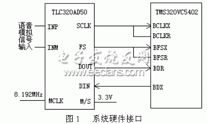
3. Interface Design In this system, the A/D data conversion chip used is the speech signal encoding and decoding chip TLC320AD50. It is a 16-bit, audio range, serial analog interface chip with anti-aliasing filters and reconstruction filters. It completes the digital sampling of the speech signal and passes the converted data to the DSP for subsequent processing.
The C5402 provides two high-speed, full-duplex, multi-channel buffered serial port McBSPs. It relies on three signals for transmitting data and receiving data: data line D (R/X), frame sync line FS (R/X), and shift clock line CLK (R/X). The DX and DR pins perform data transmission and reception when communicating with external devices, and clock and frame synchronization are controlled by CLKX, CLKR, FSX, and FSR. When transmitting data, the CPU writes the data to be sent to the transmit data register DXR, which is output by the DX pin under the action of FSX and CLKX. When receiving data, the data from the DR pin reads data from the data register DRR under the action of FSR and CLKR. CLKX, CLKR, FSX, and FSR can be generated either by an internal sample rate generator or by an external device. Set the DMA1 channel to combine with the McBSP1 channel to read the converted data of the TLC320AD50. The receiving register DRR11 (41h) of the McBSP1 channel is selected as the first address of the DMA transfer data, and the source address is selected to operate after the access is not adjusted, and the DMA channel synchronization event McBSP1 receives the event as a DMA synchronization event to implement the combination of DMA and McBSP. . The converted data of TLC320AD50 is sent to the C5402 internal receiving register DRR11 according to the setting of McBSP1, and then the DMA reads the number in DRR11 to the specified data storage area to complete the data acquisition. The DMA does not affect the normal operation of the CPU when transmitting external data. When the DMA collects a specified number of data, a DMA interrupt event is generated to interrupt the CPU to notify the CPU to perform corresponding processing. At this time, the DMA can Continue to collect the next set of data according to the settings, and realize parallel operation of data acquisition and CPU processing.
4. Software Design The system software consists of C5402 initialization program, McBSP1 initialization program, TLC320AD50 initialization program, DMA1 channel initialization program and data processing program. The C5402 initialization program completes the settings of the DSP stack, CPU clock, and operating state.
The McBSP1 initialization program sets the working state of McBSP1: when the clock is free running, the receiving/transmitting frame synchronization signal and the shift clock signal are driven by the outside world, one frame per frame, 16 bits per word, no data received or transmitted. Delay. TLC320AD50 initialization program completes TLC320AD50 related register setting: select INP/INM as analog signal input terminal, 15+1 bit ADC and 15+1 bit DAC mode, work in master mode, without slave, sampling frequency is 10.67KHz, simulation The signal input and output amplification gains are both 0dB. The DMA1 channel initialization program initializes DMA1. The specific program is as follows: ... stm #0005h, 55h ; select DMA1 channel
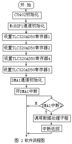
Stm #0041h, 56h ; Set the source address of the DMA event to the receiving end of the McBSP1 stm #0200h, 56h; set the destination address of the DMA event stm #0100h-1, 56h; set the number of directly transmitted data to 0100h stm #5000h, 56h Set McBSP1 to receive synchronous mode, receive one word stm #404dh, 56h in one frame; set DMA to work in multi-frame mode, source address is not adjusted, destination address is adjusted by step value of unit address index register DMIDX0 stm #20h, 55h stm #0001h, 57h ; Set the value of the unit address index register DMIDX0 to 1 stm #0282h, 54h ; set the DMA1 channel to high priority and enable the DMA1 channel...
5. Conclusion The DMA proposed in this paper combines the multi-channel buffer serial port McBSP to form a data acquisition system, which greatly reduces the workload of the CPU, simplifies the software design, effectively utilizes the hardware resources of the DSP, and improves the execution efficiency of the signal acquisition system. It has been well applied in the DSP system of our school's signal processing laboratory.
Multi-core PVC Electrical Cable
Multi-Core PVC Electrical Cable,Multicore PVC Cable,Multicore PVC Wire,Multicore Power Cable
Shenzhen Hongyan Wire Industry Co., Ltd. , https://www.hy-cable.com