Design of wireless RF transceiver system based on Si4432A This paper designs a wireless RF transceiver system based on the wireless transceiver chip Si4432 and C8051F930 single-chip microcomputer. The system consists of a sending module and a receiving module. The sending module mainly processes the data to be sent through C8051F930, and then sends it out through Si4432; in the receiving module, Si4432 displays the data after receiving it correctly through the liquid crystal, thus realizing short-range wireless communication. The system realizes high-quality wireless data transmission under the conditions of low power consumption, small size and high sensitivity. The communication between the wireless transceiver modules is sent in the form of data packets. The format of the data packet defined by this system is as follows: After the program completes the initialization of C8051F930, SPI interface and Si4432, the configuration register writes the corresponding initialization RF control word. Read the received data from the RX FIFO by accessing the register 7fh. After the corresponding control word is set, if the pin nIRQ becomes low level, it means that Si4432 is ready to receive data. After completing these initial configurations, read the packet length information through register 4bh.
This Pwm Decoder is able to accept 12-24VDC. 2811 Dmx Decoder is able to accept DC5V or DC6-24V. Led light test mode available with our decoder . The DMX to SPI converter is designed with advanced microchip technology to convert the universal standard DMX512/1990 signal into standard SPI(TTL) signal to control LED lights based on WS2801, LP6803, or similar chips. Each decoder can decode 512 channels. This compact decoder connects to DMX Devices like Luna, ISEELED DMX controller or any DMX light controller allowing its user to create endless possibilities and light shows.
Photo show of Spi Dmx Led Decoder:
Spi Dmx Led Decoder,2811 Dmx Decoder,24V Led Dmx Spi Decoder,Dmx To Spi Led Decoder Shenzhen Iseeled Technology Co., Ltd. , https://www.iseeledlight.com
1 Wireless transceiver chip Si4432
Si4432 chip is a highly integrated, low power consumption, multi-band EZRadioPRO series wireless transceiver chip launched by Silicon Labs. Its operating voltage is 1.9 ~ 3.6 V, 20-pin QFN package (4 mm × 4 mm), can work in four frequency bands of 315/433/868/915 MHz; internal integrated diversity antenna, power amplifier, wake-up timer, Digital modem, 64-byte transmit and receive data FIFO, and configurable GPIO. Si4432 requires few external components during use. A 30 MHz crystal, several capacitors and inductors can form a high-reliability transceiver system with simple design and low cost.
The receiving sensitivity of Si4432 reaches -117 dB, which can provide excellent link quality, minimize power consumption while expanding the transmission range; the minimum filtering bandwidth is 8 kHz, and has excellent channel selectivity; in 240 ~ 960 In the MHz band, the maximum output power can reach + 20dBm without the power amplifier, and the transmission and reception distance can be up to 2 km when well designed. Si4432 can be applied to many fields such as wireless data communication, wireless remote control system, small wireless network, small wireless data terminal, wireless meter reading, access control system, wireless remote sensing monitoring, hydrometeorological monitoring, robot control, wireless RS485 / RS232 data communication and so on.
2 Wireless RF transceiver system design
2.1 Overall system plan
The structural block diagram of the wireless radio frequency transceiver system is shown in Figure 1, and the Si4432 is controlled by the C8051F930 single-chip microcomputer to realize the transmission and reception of wireless data. The C8051F930 in the sending module transmits the data to the Si4432 for encoding processing and sends it to the receiving module via the antenna in a specific format. After the receiving module amplifies and demodulates the received RF signal, it sends the data to the main controller C8051F930 for corresponding processing, such as LCD display. The system provides human-computer interaction interfaces such as buttons and liquid crystal (OCM12864-9), and RS232 interface is also left to communicate with the PC. 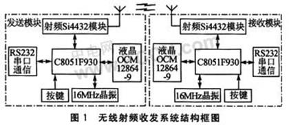
2.2 System hardware design
The main control chip selects the single-chip microcomputer C8051F930 from Silicon Labs. The C8051F930 has 4 KB of RAM and 64 KB of Flash. On-chip integrated rich peripheral modules (including serial port, SPI, 10-bit A / D converter, etc.), which satisfactorily meet the requirements of the system for microcontrollers; support Quick wake-up and minimum 0.9 V power supply; there are multiple power management modes (such as normal mode, idle mode, sleep mode, etc.), the two built-in undervoltage detectors integrated are suitable for sleep mode and normal mode, typical sleep In mode, the current is only 50 nA. The C8051F930 contains a high-efficiency DC boost converter that provides up to 65 mW to the internal microcontroller and other components. To reduce battery consumption in normal mode, the power-saving architecture of the C8051F930 can reduce the current in operating mode. To 170μA / MHz.
C8051F930 can read and write internal registers of Si4432 through built-in enhanced SPI, and flexibly configure various parameters. Through the SPI interface to complete the initial configuration of Si4432, read and write data, access FIFO and other operations. Use 4-wire SPI, namely MOSI, MISO, SCK and nSEL. MOSI is used for serial data transmission from C8051F930 to Si4432; MISO is used for serial data transmission from Si4432 to C8051F930; SCK is used to synchronize serial data transmission between C8051F930 and Si4432 on the MOSI and MISO lines; nSEL is used as a chip Select signal, only when the chip select signal is low level, the operation of Si4432 is effective. The hardware design schematic is shown in Figure 2. 
Pins 13 to 16 of Si4432 are standard SPI interfaces, and pin 17 (nIRQ) is an interrupt status output pin. When FIFO overflow, valid data packet transmission or reception, CRC error, detection of preamble and sync word, power-on reset, etc., and the corresponding interrupt is enabled, pin 17 will generate a low level to notify C8051F930 has an interrupt. 20 feet (SDN) determines the working state of Si4432 chip. When SDN is grounded (SDN = 0), the chip is in the normal working mode; when connected to a high level (SDN = 1), the chip is in the power-down mode. The contents of the register will be lost in power-down mode, and SPI access is not allowed, but the current consumption of the chip is only 10 nA, and the power consumption is very low, so it is suitable for applications that require very low power consumption. After connecting to the power supply, power-on reset on the falling edge of SDN and switch to other operating modes according to the instructions.
In order to achieve a better communication effect, the resistance and capacitance parameters of the matching circuit of the receiving low noise amplifier and the matching circuit of the transmitting power amplifier of the Si4432 should be selected in strict accordance with the parameters provided in the data sheet. The diversity circuit of the front end adopts SKY13267, and its V1 pin and V2 pin are connected to GPIO1 and GPIO2 of Si4432 respectively. Through this crossbar switch, the automatic switching of the transmit and receive channels of the diversity antenna is realized.
2.3 System software design
The software programming adopts the modular design idea, and each main function module in the system is compiled into an independent function to be called by the main program. Function modules include: initialization procedures (including initialization of C8051F930, SPI, Si4432), wireless transmission procedures, wireless reception procedures, etc. The wireless transmission program is responsible for writing the data payload, and adds the preamble, synchronization word, data payload length and CRC check byte to the data payload according to the communication protocol to form a data packet and sends it; the wireless reception program is responsible for receiving and verifying the data CRC bytes in the packet to ensure the accuracy of the received data. ![]()
Among them, Preamble (preamble) is a series of 10101010, the number of which is 8n bits, and the size of n is determined by user programming. In the process of data packet transmission, a preamble with a set length is added in front of each packet; in order to recognize the arrival of a frame, the receiving end needs the preamble to perform frame synchronization to determine when to send and receive data between the receiving and sending systems. SyncWord (synchronization word) after the preamble, you must use the set synchronization word as the synchronization code. The synchronization word set by this system is 2 bytes, and the content of the synchronization word is 0x2DD4. The receiving end starts to receive data after detecting the synchronization word. Packet Length is the length of the data payload. PAYLOAD (payload) is the data sent by the user. The CRC (CRC checksum) is checked by the built-in CRC. Si4432 integrates functions such as modulation / demodulation, encoding / decoding, etc., so Prearnble, SyncWord, Packet Length and CRC are automatically added by the hardware. The user only needs to set the specific structure of the data packet and part of the structure (such as Preamble and sync word).
This article takes half-duplex communication as an example to introduce the implementation process of communication. The programming environment is Silabs IDE V3.61, and the test passed in this compilation environment. Silabs IDE integrates source code editing, program source code level debugger and in-system Flash programmer. Also supports the use of third-party compilers and assemblers,
(1) Initialization procedure
The initialization procedure includes the initialization of C8051F930, the initialization of SPI, and the initialization configuration of Si4432's internal registers such as wireless transceiver frequency, working mode, and transmission rate.
After the system is powered on, the C8051F930 is in the default state, and the initial configuration is re-configured according to the system functional requirements. The digital crossbar switch of C8051F930 allows internal digital system resources to be mapped to port I / O pins. The on-chip resources can be configured to specific port I / O pins by setting the crossbar control register. This feature allows users to choose the combination of general-purpose port I / O and required digital resources according to their specific application, which increases the flexibility of the application. In this system, it is mainly configured with 4 lines of SPI communication, data line interface of LCD, control line interface and RS232 serial port data input / output, etc.
When initializing the SPI, you can choose the specific usage rules through the configuration of the SPIlCFG register and SPIlCN register. Here, select the main SPI, 4-wire mode, the clock polarity is low, and the data is sampled at the rising edge of the clock; by configuring the SPIlCKR register, the synchronous clock frequency can be set to 1/4 of the crystal frequency.
At the beginning of power-up, Si4432 is also in the default state and needs to be configured to work. Si4432 has more than 70 registers that need to be configured. They determine the working mode of Si4432. For specific configuration, please refer to Si4432 data sheet. The initialization of Si4432 is an important part. The proper configuration has a great influence on the final communication effect of the system. The main controller C8051F930 configures Si4432's 1ch, 1dh and other registers through SPI, writes the corresponding initial RF control words (mainly frequency, transmission speed, transmission method, etc.); configures the structure and preamble of the packet by configuring 33h, 34h and other registers Code length, sync word content, etc. This system adopts the synchronous transmission mode, with 0x2DD4 as the synchronous mode mark code, and the data load is not transmitted until the synchronization word is transmitted. Every time the data is sent, the synchronization word 0x2DD4 must be used as the synchronization flag to send the data. The receiving end starts to receive the data after detecting the synchronization word.
(2) Wireless transmission program
The wireless sending procedure flow is shown in Figure 3. After the initialization of C8051F930, SPI and Si4432, the corresponding initialization RF control word is written in the configuration register. Next, set the length of the packet by configuring the register 3eh of Si4432, write register 7fh continuously through SPI, and write the data to be sent to the TX FIFO. Then turn on the "Send Interrupt Enable" flag to disable other interrupts. When a data packet is sent, the pin nIRQ will be pulled low to generate a low level to notify the C8051F930 that the data packet has been sent. After the interrupt is enabled, the transmission function is enabled and the data starts to be transmitted. Wait for the nIRQ pin to be pulled low due to interrupt generation. When the nIRQ pin becomes low, read the interrupt status and pull nIRQ high, otherwise continue to wait. If the data is sent successfully, the indicator will turn on. After a successful data transmission, it enters the next data cycle transmission state. 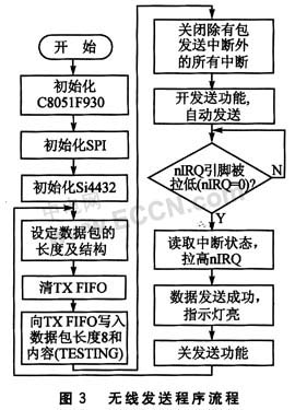
(3) Wireless receiving program
The wireless receiving program flow is shown in Figure 4. 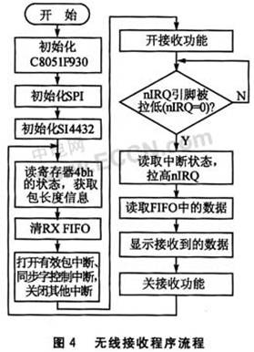
Then, turn on "active packet interrupt" and "sync word detection interrupt" to disable other interrupts. Pin nlRQ is used to detect whether a valid packet has been detected. If pin nIRQ goes low, it means that a valid data packet has been detected. This system uses 0x2DD4 as the mark code of the synchronization mode. The receiving module detects the synchronization word to receive data synchronously.
Finally, the receiving function is enabled and the data starts to be received. Wait for the nIRQ pin to be pulled low due to interrupt generation, read the interrupt flag bit to reset the nlRQ pin, and restore nIRQ to the initial high state to prepare for the next interrupt triggered detection. Read the data in the RX FIFO through SPI, send the data to the LCD OCM12864-9 display, and then enter the next data reception state.
3 PCB design considerations
PCB design has a great influence on the performance of the entire system. The following are the points to note when designing Si4432 PCB:
â‘ In order to eliminate the inductive effect of the routing problem, as many vias as possible should be arranged in the free space on the PCB. In order to achieve a better radio frequency communication effect, the entire PCB should be covered with copper. When a better RF ground is provided, the grounded copper area in the TX / RX area helps reduce or even avoid radiated interference.
â‘¡Decoupling capacitors should be added at the power access end, and as close as possible to the Si4432 chip. The filter capacitor should also be as close as possible to the corresponding pin, so that you can get better filter performance.
â‘¢Si4432 has few peripheral components, so small 0402 packaged chip devices should be used as much as possible. Among them, the inductance belongs to the key device, need to select the high-accuracy inductance.
④ The Si4432 choke inductor L1 should be as close as possible to the Tx pin; the inductor L2 connected in parallel on RXn and RXp should be vertically arranged on the PCB plane, and the directions of the inductors L1, L3, L4, L5 on the Tx channel should be perpendicular To reduce coupling; the unrouted area between the Tx channel and the RXn / p channel should be isolated with grounded copper clad, and the wiring area of ​​the Tx channel matching circuit should not occupy too much board area as much as possible.
⑤ The selection of crystal oscillator refers to the following parameters: the equivalent series resistance is 60 Ω, the load capacitance is 12 pF, and the frequency accuracy is ± 20 × 10-6. Keep the crystal oscillator and the chip's crystal oscillator access pins as close as possible, and isolate the clock area with a ground wire.
â‘¥ When designing the PCB, the bottom of the Si4432 chip in QFN package is grounded. Drill 9 12 mil (1000 mil = 25.4 mm) ground vias on the bottom of the Si4432 chip to ensure good grounding and heat dissipation capabilities and enhance communication reliability.
⑦ The traces on the board should not pass through the Tx / RXn / p area as much as possible to prevent the coupling effect of the matching network.
4 System testing and analysis
In order to verify the reliability of the design of this radio frequency transceiver system, 7 sets of "transmit module-receive module" communication experiments were carried out. When the communication distance in the open ground is about 1500 m, 7 groups of “transmit module-receive module†work on 7 central frequencies such as 430.50 MHz, 431.50 MHz, and 432.50 MHz respectively, the bandwidth is 112.8 kHz, and the frequency offset is ± 25 kHz, sending 4 000 data packets, the experimental results are listed in Table 1. 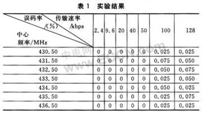
It can be seen from Table 1 that when the transmission rate is low, the bit error rate is 0; when the transmission rate is 100 kbps (or above), there are certain bit errors, but the bit error rate is less than 0.075%. Therefore, the wireless radio frequency transceiver system has the characteristics of long transmission distance, strong wall penetration capability, and low communication error rate.
Conclusion
This system can be fully expanded into a network system to form a wireless network for application to field control or measurement and control systems. The radio frequency transceiver system designed in this paper is reliable, stable, and has good versatility. It can be applied to other short-range wireless communication fields such as cell paging, industrial data collection, biological signal collection, wireless remote control, etc. with minor modifications. The higher market application value provides a good solution for wireless data transmission. 