FA5310 switching power supply control IC and its application
Many electronic systems require switching power supplies. The circuit of the switching power supply is diverse, and many of them have adopted the control chip. As long as the control chip is connected with some other devices, it can form a switching power supply, which greatly simplifies the circuit design.
FA5310 is a product of Fuji Electric Co., Ltd. of Japan. It has multiple protection functions, simple external circuits, and great practical value. FA5310 has the following characteristics:
Can directly drive the power MOSFET (I0 = ± 1.5A); wide operating frequency range (5 ~ 600kHz); with pulse-by-pulse over-current limit function; with overload cut-off function (lock or no protection mode can be selected); can be controlled by external signal Output ON / OFF; with over-voltage cut-off function (in lock mode) and under-voltage malfunction protection function (on at 16V, off at 8.7V); low waiting current (90μA); duty cycle is Dmax = 46 % Can be used in forward and flyback circuits.
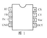
Fig. 1 is the pin arrangement diagram of FA5310. Table 1 lists the functional description of each pin.
2 working principle
The working principle of FA5310 is as follows.
2.1 Oscillator
The oscillator generates a triangle wave by charging and discharging the capacitor. The voltage of the CT pin oscillates in the range of about 3.0V to 1.0V. The oscillation frequency is determined by the external time base resistance RT and time base capacitance CT of pins 1 and 7. The following formula:
In the formula, the unit of f is kHz, RT is kΩ, and the unit of CT is pf.
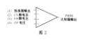
2.2PWM comparator
The PWM comparator has four input terminals (as shown in Figure 2). The oscillator output (1) is compared with the CS pin voltage (2), FB pin voltage (3) and DT voltage (4). If the minimum value of pin (2) (3) (4) is lower than that of pin (1), the PWM comparator output is high and the IC output is low; otherwise, the PWM comparator output is low and the IC output It is high level.
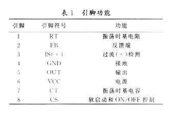
Figure 3 is a timing diagram of the PWM comparator. When the IC is powered, the CS pin voltage can be used to control the soft-start operation, and the output pulse gradually widens. In normal operation, the output pulse width depends on the maximum duty cycle Dmax, DT voltage and FB pin voltage.
2.3 CS pin circuit
CS pin can be used for soft start operation, overload and overvoltage output shutdown and output ON / OFF control.
(1) Soft start function
When the power is turned on, a constant current source of 10 μA starts to charge the capacitor Cs. The CS pin voltage rises slowly due to charging. Therefore, the output pulse of the PWM comparator also gradually widens.
The soft-start time can be estimated approximately from the time the IC is started until the output pulse becomes 30% wider. The soft start time is given by the following formula: ts (ms) = 160Cs (μF)
(2) Overload shutdown
If the output voltage drops due to overload or short circuit, the voltage at the FB pin will rise. If the voltage of the FB pin exceeds the reference voltage of the comparator C3 (2.8V), the output of C3 is a low level, which will turn off the transistor Q. In normal operation, the transistor Q is turned on. The CS pin is clamped at 3.6V by the voltage regulator Zn. The maximum breakdown current of this regulator is 65μA. When Q is turned off, the clamp is released, the constant current source of 10μA starts to charge the capacitor CS, and the CS pin voltage rises. When the voltage of the CS pin exceeds the reference voltage of the comparator C2 (7.0V), the output of C2 is a high level, thereby turning off the bias circuit. In this way, the IC enters the lock mode and shuts down the output. The consumption of the shutdown current is 400 μA (Vcc = 9V). This current must be provided by the starting resistor. At this time, the IC starts to discharge the MOSFET gate.
The circuit can be restarted when the power supply voltage Vcc drops below 8.7V or the CS pin voltage is forced to fall to 7.0V. The time period tOL from the output short circuit to the turn-off bias circuit is given by:
tOL (ms) = 340Cs (μF)
(3) Output ON / OFF control
If a triode is connected in parallel next to the capacitor Cs, and the CS pin voltage is controlled by controlling the on and off of the triode, the on or off of the IC can be controlled.
If the transistor is turned on and the CS pin voltage drops below 0.42V, the C1 comparator output high level turns off the bias circuit, thereby turning off the IC output, and the IC discharges the MOSFET gate. If the transistor is cut off, Cs starts to charge again, and the IC starts soft-start. The power supply started working again.
2.4 Overcurrent limit circuit
The overcurrent limiting circuit limits the overcurrent by detecting the pulse-by-pulse peak value of the drain current of the main switching MOSFET. The threshold voltage of detection is + 0.24V.
The MOSFET drain current is converted into a voltage by the resistor R2 (see Figure 4) and fed back to the IS pin. If the voltage exceeds the reference voltage of the comparator C4 (0.24V), the output of C4 is high, and the output Q of the RS flip-flop is also high, then the output pin quickly turns off the current. The output Q of the RS flip-flop is reset in the next cycle of the oscillator, so that the output terminal starts to work again. This work is repeated to limit overcurrent. If the over-current limit acts due to noise, an RC filter can be connected between the IS pin and the MOSFET.
2.5 Undervoltage lockout circuit
When the power supply drops, the undervoltage lockout circuit in the IC can prevent the IC from malfunctioning. When the power supply voltage starts to rise from 0V, the IC starts working when Vcc = 16.0V. When the power supply voltage drops to Vcc = 8.7V, the IC turns off the output. When the undervoltage lockout circuit works, the CS pin voltage becomes low, resetting the IC. 2.6 Output circuit
The IC's push-pull output can directly drive the MOSFET. The current of the OUT pin can reach 1.5A.
During the operation of the undervoltage lockout circuit, if the IC stops working, the MOSFET gate voltage drops and the MOSFET is turned off.
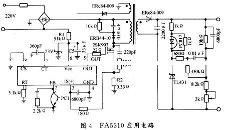
3 Application circuit and design considerations
Figure 5 shows the application circuit of FA5310. The time from power-on to IC start-up is determined by R1 and C5. If they are too large, the circuit will start more slowly. R1 must be determined according to the following formula. Considering that the current when the circuit is off is 400μA (when cc = 9V):
R1 <{VAC (2) 1/2 / 2Ï€-9} / 400AC is the AC input voltage.
When the IC power supply circuit starts, it is powered by the power supply through R1, but the current is small. After the circuit works normally, the feeder winding of the transformer is rectified by the diode ERA91-02 to supply power to the IC, so that the current required by the IC can be guaranteed. The auxiliary source can also be omitted. Because the MOSFET has to withstand twice the peak voltage of the power supply, the fluctuation of the power grid and the surge voltage, so for 220V grid voltage, the MOSFET's withstand voltage should be preferably above 800V. The RCD circuit on the drain of the MOSFET is a reset circuit, and the RC circuit between the source and drain is used to suppress the surge voltage.
In the transformer secondary, when the output voltage is much higher than 5V instantaneously, the optocoupler PC1 is turned on, making the FB terminal short to ground, the IC suspends the output, from
And keep the circuit output stable.
Significant product benefits:
1)A full line of spools in a variety of standard sizes
2)High speed custom labeling and printing on flanges available – even on short runs
3)One piece molded construction for strength and precision
4)Appealing designs as well as ergonomics (no sharp edges)
|
Type
|
Weight
(gram)
|
d1
(mm)
|
D1
(mm)
|
d2
(mm)
|
D2
(mm)
|
H1
(mm)
|
H2
(mm)
|
d3
(mm)
|
A1
(mm)
|
A2
(mm)
|
d4
(mm)
|
E
(mm)
|
|
PC-70
|
40
|
70
|
38
|
70
|
85
|
20
|
7
|
7
|
|
|
|
PC-80
|
70
|
80
|
50
|
64
|
80
|
20
|
8
|
8
|
7
|
20
|
|
PC-83
|
70
|
83
|
45
|
100
|
120
|
20
|
10
|
10
|
|
|
|
PC-100A
|
110
|
100
|
45
|
70
|
88
|
20
|
9
|
9
|
|
|
|
PC-100B
|
100
|
100
|
45
|
100
|
120
|
20
|
10
|
10
|
|
|
|
PC-125A
|
180
|
125
|
65
|
100
|
120
|
20
|
10
|
10
|
7
|
20
|
|
PC-125B
|
170
|
125
|
70
|
100
|
120
|
20
|
10
|
10
|
|
|
|
PC-130A
|
200
|
130
|
65
|
100
|
120
|
22/25
|
10
|
10
|
|
|
|
PC-130B
|
210
|
130
|
65
|
100
|
120
|
22
|
10
|
10
|
|
|
|
SH-16
|
230
|
150
|
90
|
100
|
124
|
30
|
12
|
12
|
12
|
26
|
|
PC-185A
|
400
|
185
|
128
|
155
|
178
|
30
|
11
|
11
|
|
|
|
PC-185B
|
500
|
185
|
128
|
155
|
178
|
30
|
11
|
11
|
|
|
|
PC-185C
|
500
|
185
|
130
|
160
|
180
|
30
|
10
|
10
|
|
|
|
PC-220A
|
660
|
220
|
110
|
155
|
185
|
40
|
15
|
15
|
12
|
42
|
|
PC-220B
|
660
|
220
|
110
|
155
|
185
|
38
|
15
|
15
|
15
|
38
|
|
PC-220C
|
660
|
220
|
110
|
155
|
185
|
30
|
15
|
15
|
14
|
38
|
|
PC-250
|
870
|
250
|
110
|
155
|
185
|
40
|
15
|
15
|
12
|
42
|
|
PC-300A
|
1400
|
300
|
180
|
170
|
200
|
32
|
15
|
15
|
17
|
45
|
|
PC-300B
|
1400
|
300
|
180
|
170
|
200
|
100
|
15
|
15
|
20
|
125
|
|
PC-355
|
1950
|
355
|
224
|
160
|
200
|
36
|
20
|
20
|
26
|
50~80
|
|
PC-410
|
4550
|
410
|
310
|
180
|
228
|
70
|
24
|
24
|
|
|
|
PC-500A
|
8450
|
500
|
315
|
180
|
250
|
40
|
35
|
35
|
26
|
70~100
|
|
PC-500A1
|
8450
|
497
|
315
|
180
|
250
|
40
|
35
|
35
|
26
|
70~100
|
|
PC-500B
|
8600
|
500
|
250
|
250
|
300
|
56
|
25
|
25
|
26
|
70~100
|
|
PC-500B2
|
9020
|
500
|
250
|
240
|
290
|
40
|
25
|
25
|
26
|
70~100
|
|
PC-500C
|
8600
|
500
|
250
|
235
|
300
|
56
|
20
|
20
|
26
|
70~100
|

Wire Packaging Spool
Wire Packaging Spool, Magnet Wire Reel, Magnet Wire Spool, Packing Wire Spool
NINGBO BEILUN TIAOYUE MACHINE CO., LTD. , https://www.spool-manufacturer.com
