Dual Voltage Tracking Circuit
Principles covered include: the need for tracking, pracTIcal circuits, controller funcTIons, selecTIon of tracking voltage levels, component value selecTIon, overall circuit accuracy, circuit stability, the characteristics of some commercially-available DC / DC converters, and cascaded supply and parallel supply operation. Circuits are provided with options and tracking waveforms. A component-selection spreadsheet for calculating component values ​​(Excel, 196KB) is available
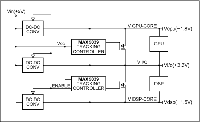
Figure 1. Basic dual voltage-tracking control.
When VI / O comes up before VCORE, VCORE is derived from the higher VI / O voltage with the controller and MOSFET operating as a series regulator. When VCORE comes up before VI / O, the VI / O is connected to the VCORE voltage with the controller and MOSFET operating as a series switch. It may be preferable that the VI / O supply come up slightly before the VCORE supply, but it is not a requirement (depends upon supply characteristics).
Detailed CircuitA complete single-channel voltage-tracking circuit with all options appears in Figure 2. This circuit contains the full-featured MAX5040 providing a power-OK or POK output. The open-drain POK output is released to go HIGH when the voltage at I / O SENSE <1.230V and the tracking phase is completed. The component functions are as follows:
Q1, NMOS-shunt switch or regulator
C1, C2 & R3-regulator control-loop compensation
R1 & R2-feedback voltage-control attenuator sets VCORE tracking voltage
R9 & C3-feedback lead network
R5 / R6-power-OK sense setpoint attenuator
D1 & CIN-energy storage allows controller to continue functioning while power shuts down
R7 & R8-startup-voltage setpoint attenuator.
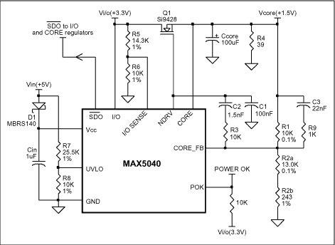
Figure 2. Complete voltage tracking circuit for a single core voltage.
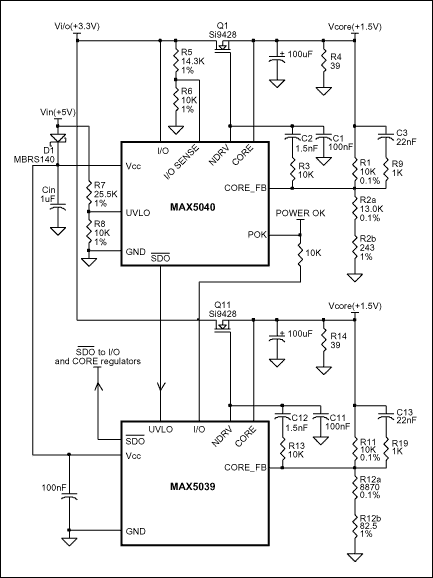
Figure 3. Dual tracking controller circuit for two core voltages.
Note that only a single UVLO resistor divider is used. The / SDO \ output of the first controller is connected to the UVLO input of the next controller in daisy-chain manner, and / SDO \ of the final controller in the series is used to enable all low-voltage regulators. Each R1 / R2 divider is adjusted for the required tracking core voltage. If MAX5040 controllers are used, each POK output may be used independently or collector ORed to provide a single composite POK if desired. Otherwise, a single MAX5040 could be used while the remaining controllers are MAX5039.
Controller Turn-On OperationThe MAX5039 / MAX5040 tracking controller is powered by VCC from a 5V control supply line. The following explanations assume that the VI / O enable signal precedes the VCORE enable signal. [Differences are noted for situations when the two enable signals are coincident or when VCORE enable preceeds VI / O enable.] Startup operation is initiated when Vcc is applied (either ramped or stepped up from zero). Refer to Figure 4.The IC becomes active when Vcc reaches 0.9V, at which time the active-low regulator-shutdown line / SDO \ is driven LOW to insure that the VI / O and VCORE supply regulators are disabled.
When VCC reaches 2.5V, NDRV is driven to VCC, turning ON the low-threshold MOSFET to connect the VI / O and VCORE lines together. The supply regulators are still OFF because / SDO \ remains LOW.
When VCC reaches
VI / O precedes VCORE, and begins to rise at a rate determined by the I / O regulator characteristics. NOTE: Neither VI / O nor VCORE should rise at a rate exceeding 6.6V / µs. VCORE rises with VI / O because the two regulator output lines are connected via the MOSFET. During this phase, the I / O regulator output supplies both the I / O and CORE loads and backdrives the CORE regulator output; both voltages are equal. [If VCORE precedes VI / O, VCORE backdrives the VI / O supply; both voltages are equal. Refer to Figure 5.]
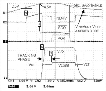
Figure 4. Startup / shutdown operation, VI / O enable preceeds VCORE enable.
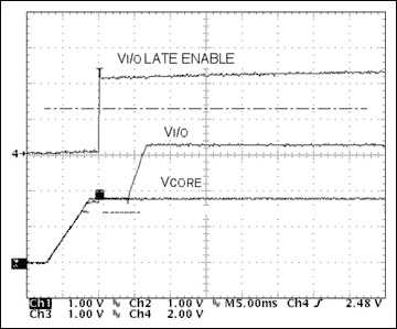
Figure 5. Startup operation, VCORE enable preceeds VI / O enable.
The controller and MOSFET act as a series-pass regulator until VCORE becomes available when VCORE rises to its normal regulator-controlled level, NDRV is driven LOW to turn OFF the MOSFET, the two voltages become independent, VI / O rises to its normal level , and the controller turn-on sequence is terminated.
If the turn-on sequence is delayed because either VI / O or VCORE does not come up within an internally-timed 15ms after / SDO \ is released, / SDO \ will be driven LOW to abort the turn-on sequence. This fault condition is latched to prevent an automatic restart attempt. Controller Turn-Off OperationDuring normal operation, the controller continually monitors the CORE, I / O and CORE_FB voltages. If VCORE drops to the core regulation voltage set by R1 / R2 (perhaps due to an unexpected high-current load or a short), NDRV will be driven high to re-assert the regulation mode. Refer to Figure 4.
If this condition lasts beyond the 10-20ms fault time-or if the voltage on the UVLO pin drops below its threshold voltage, / SDO \ will be driven LOW to begin a shutdown operation.
VUVLO drops below the UVLO threshold, or a fault lasts beyond 10-20ms./ SDO \ is driven LOW to disable the VI / O and VCORE supplies.
An internal 20W MOSFET bleeder between VCORE and ground is turned ON to discharge the output loads.
VCORE begins to drop.
VCORE drops to the VCORE set point while VI / O remains higher than VCORE, NDRV is driven to an intermediate point as needed to regulate VCORE at the set point so long as VI / O remains greater than VCORE.
VI / O drops to VCORE, NDRV is driven to VCC, turning ON the MOSFET to short the VI / O and VCORE lines together. Note: It is important that Vcc remain in its operating range during the power-down stage so that the controller can continue to control NDRV until the loads are discharged [1]. Selecting the Core-Voltage Tracking LevelThe core-voltage tracking level [2] VCT-set by feedback attenuator R1 / R2 in Figure 2-is that voltage at which VCORE is held while the controller is in tracking mode. This occurs when the VI / O supply comes up before the VCORE supply. Selection of the core-voltage tracking level is an important consideration that depends primarily upon the VCORE and VI / O supply accuracies. The constraints are as follows:
VCT must be below the tolerance-limit value of VCORE, VCT must be above VI / O minus the allowed differential between VI / O and VCORE, VCT cannot be above VI / O, or VCT must be above the minimum allowed VCORE. We must know in advance the limits on the VI / O and VCORE supplies.
As an example, we set the following limits:
VI / O supply = 3.3V ± 5%, or 3.135-3.465V,VCORE supply = 1.5V ± 50mV (± 3.33%), or 1.45-1.55V,
VCORE minimum voltage = 1.5V-10%, or 1.35V, and
VCT must then be in the range 1.35-1.45V including all setting errors.
Attenuator R1 / R2 ratio is chosen such that 0.8V appears on the CORE_FB pin during the tracking phase. We will use VCT = 1.40V in the example.
Core voltage and VCT error limits of from all sources are shown in Figure 6. The VCT must be kept above 1.35V minimum VCORE allowed and below 1.45V minimum VCORE supply range.
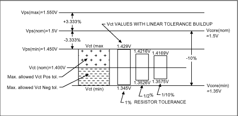
Figure 6. Representation of VCT error limits and realized values.
The resistors themselves have tolerance; suggested resistor tolerance is ± 0.1%.
The resistors have a temperature coefficient, ± 25ppm / ° C for 0.1% and 0.5% resistors and ± 100ppm for 1% resistors.
Resistor selection may only be made in 1-2% increments.
CORE_FB bias current could have an effect if R1 and R2 are of very high value.
The internal control amplifier has a limited gain, so the calculation of R1 / R2 ratio includes the effects of finite amplifier open-loop gain. The complex calculation can be ignored in selecting R1 / R2, and an error term can be derived. But, Don't PanicWe can simplify all of this for you and mechanize the process of selecting R1 / R2 values. Actually, the prime contribution to error is the ± 2% of the reference itself. So let's inspect each item, one at a time to see how much each contributes to the total error. All resistor-value related errors are influenced by the R1 / R2 ratio so vary with the selected VCT. The MAX5039 / MAX5040 Component-Selection Spreadsheet
http://pdfserv.maxim-ic.com/arpdf/MAX5039/vset.zip
performs all error calculations at any allowed R1 / R2 ratio; it also mechanizes selection of the UVLO and I / O sense resistor attenuators (see Figure 2).
Many readers may prefer to skip over the following section as it is presented primarily as an aid to understanding how the Component-Selection Spreadsheet is mechanized.
Reference ErrorThis is a real ± 2% and cannot be reduced.
Resistor Tolerance
Resistor tolerance error is not a fixed value independent of the R1 / R2 ratio, but is a function of this ratio. Using ± 1% resistors is not recommended. Using ± _% resistors is similar in cost to using ± 0.1% resistors, so ± 0.1% resistors are recommended. Calculated worst-case tolerance errors are ± 0.0857% at VCT = 1.40V (
 = 0.57143).
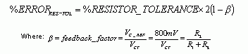
The TCR is stated as ± and shown as a typical butterfly curve, so worst case is when one resistor exhibits a positive TCR while the other exhibits a negative TCR. In fact, resistors of equal value would be expected to exhibit nearly identical TCR; and the values ​​of R1 and R2 will differ by less than 2: 1. Assuming that similar valued resistors will track to ± 10ppm, calculated worst-case TCR errors for ± 25ppm resistors over a temperature range of -40 to + 85 ° C are ± 0.056% at VCT = 1.40V. The spread sheet, however, accepts ± 25ppm as a real value for 0.1% resistors (± 0.1398% over temperature at 1.40V). Resistor TCR error may be calculated according to the formula:
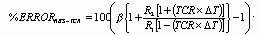
TCR is expressed in parts per million, but should be written as a decimal fraction in the equation (eg; 25ppm = 0.000025).  T is the absolute value of the greatest difference from 25 ° C (eg; -40 to + 85 ° C yields two values: -65 ° and + 60 °).
A similar value applies when the (+) and (-) are reversed in the above quotient.
Resistor SelectionAlthough available resistor values ​​are in
The data sheet listing of 300nA max over temperature is selected to allow a short test time, and does not represent the actual leakage current, which is less than 30nA at 85 ° C. One to thirty nanoamp flowing in R1 (10K) (refer to Figure 7) would cause an error of 10-300µV (+0.0007 to + 0.021% of VCT), so may be ignored in the error calculation. No negative error is possible in this calculation.
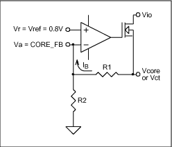
Figure 7. Tracking-voltage control loop.
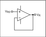
Figure 8. Reference voltage measurement circuit.
Closed-loop-gain error calculation is somewhat elusive in this case because the given reference-voltage error includes its own loop-gain error due to being measured at the op-amp output when set at unity closed-loop gain. Actual open-loop gain of the op-amp itself is typically 4000, but ranges from 1000 to 10,000 [4]. The MOSFET source-follower gain is> 0.99 due to the extremely high NMOS gfs, so overall loop gain is nearly unchanged. Normally the closed- loop loop gain of the circuit in Figure 7 is calculated as:
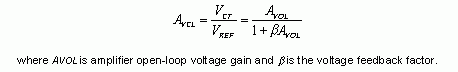
Appropriate mathematical manipulations can be applied to show that, due to the VREF measurement and specification method used in Figure 8 where VREF is measured as VR, but is suggested to be located at VR0, the corrected gain equation is:
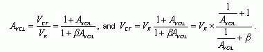
Error can be calculated by forming a ratio of actual to ideal, subtracting 1, and multiplying x100 for percentage. The final form of the VCT equation above collapses to 1 / when Avol = , therefore the error at minimum gain is:
Real calculated worst-case open-loop gain error is -0.00075 to -0.0749% at VCT = 1.40V. No positive error is possible in this calculation.
Error Linear SumCalculated worst-case error sum with 0.1% resistors (including 300µV CORE_FB bias error, 25ppm TCR, and 0.01% resistor-selection error) is -2.316 / + 2.257% at VCT = + 1.40V. The MAX5039 / MAX5040 Component-Selection Spreadsheet calculations include all possible errors except the CORE_FB bias-current error. Circuit Stability ConsiderationsComponents C1, C2, and R3 in Figure 2 control the tracking regulator amplifier stability, and are fully described in the MAX5039 / MAX5040 data sheet. It is suggested that the feedback resistor R1 be chosen as a constant value (with adjustment provided by variation of R2). This allows C2 and R3 to remain fixed in value without regard to the VCT value selected [5]. The Component-Selection Spreadsheet calculates these values ​​for any chosen value of R1.
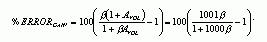
Lead network C3 / R9 improves tracking-loop speed to eliminate VCT overshoot and undershoot during the tracking phase. Figures 9 and 10 illustrate the improvement with the lead network in place. Note the NDRV slow response and overshoot without the lead network and the resultant VCT overshoot and undershoot in Figure 9 (vertical scales differ in the two figures). The Component-Selection Spreadsheet calculates these values ​​for any chosen value of R1.
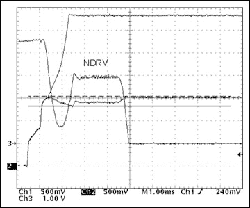
Figure 9. Startup waveforms without lead network.
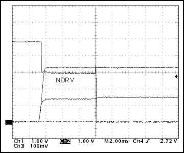
Figure 10. Startup waveforms with lead network.
Resistor R4 may remain fixed without regard to the value of CCC when the lead network is in place. R4 = 39 works well with CCC values ​​to 1500µF or more. For very large values ​​of CCC, one might consider reducing R4 for slightly-improved loop stability in the tracking phase.
Dual-tracking-control startup and shutdown waveforms appear in Figures 11 & 12.
Figure 11. Dual tracking startup waveforms.
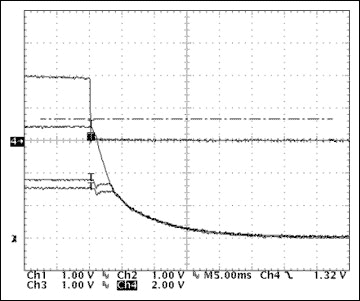
Figure 12. Dual tracking shutdown waveforms.
We will consider 3 basic configurations described as systems A, B, and C, and diagrammed in Figure 13 with variations to be described later.
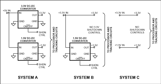
Figure 13. Three basic power system source configurations.
The main difference in how to treat the tracking-control circuits is based on the availability of shutdown-control signal inputs to the converters and upon the characteristics of the converters themselves. System-A has shutdown-control signal inputs available, while system B has no shutdown control available for the + 3.3V VI / O, and system C has no shutdown control available on either the VI / O or VCORE supplies.
Systems B and C must include a series switch to interrupt and control one or more of the voltage sources. It has been previously mentioned that 6.6V / µs is the maximum voltage rate of rise acceptable to the MAX5039 / MAX5040 tracking controllers. The system processor specification may also restrict the maximum rate of rise for its VI / O and VCORE voltages. In these cases, the series switch must have the capability of controlling output voltage rate of rise. This is easily achieved when the tracking controller is augmented with a single MAX6820 power-supply sequencer IC plus a series MOSFET for each non-enabled supply.
In addition, we need knowledge of the DC-DC converter enable-controlled voltage rate of rise and over shoot, polarity of the enable control, and any enable sequencing requirements. Enable sequencing requirements may come about if the converter / regulator misbehaves when its output is backfed from another voltage source at start up, or if the first converter to come up cannot support the entire system startup current including capacitor charging. In most cases it is desirable to delay the VCORE enable signal by _-2ms after the VI / O enable signal.
The power converters may be easily constructed using MAX1842 to meet required voltage rate of rise and overshoot characteristics, or modular converters may be purchased ready made. Some modular power converters like the Power Trends PT6600 series may require series MOSFET switching to control voltage rate of rise because of exhibited excessive enable-controlled output-voltage rate of rise and overshoot. Others like the DATEL LSN series exhibit nicely-controlled voltage rate of rise without overshoot, but may require staggered enable signals to ensure proper startup operation. The PT6600 series has positive -logic enable control, while the LSN series has negative-logic enable control. Table 1 lists some options.
Table 1. Some Modular and Built-Up Converter Characteristics
| CONVERTER TYPE AND SERIES | DISABLE SIGNAL POLARITY | ENABLE SEQUENCING REQUIRED | ENABLE-CONTROLLED OUTPUT VOLTAGE RATE OF RISE | ENABLE-CONTROLLED OUTPUT VOLTAGE OVERSHOOT |
| MAX1842 Discrete | Negative | Suggested with single R / C delay | Controlled | Controlled |
| DATEL LSN Series | Positive | Suggested with single R / C delay | Controlled | Controlled |
| Power Trends PT6600 Series | Negative | Not applicable because of  | Uncontrolled. Hardwire enable ON, and control input-voltage slew rate | Uncontrolled. Hardwire enable ON, and control input-voltage slew rate |
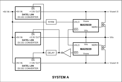
Figure 14. Parallel type-A system also illustrating delayed and inverted ENABLE.
Discrete converters built with the MAX1842 will operate in the ciruit of Figure 15 without inverters in the enable line.
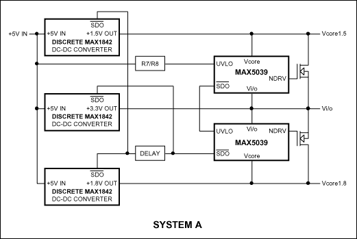
Figure 15. Parallel type-A system with discrete converters.
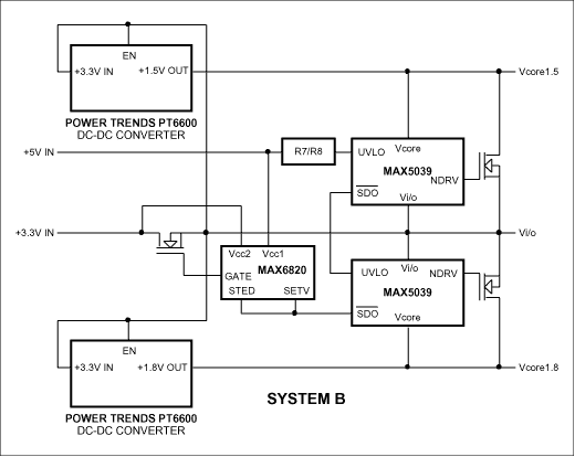
Figure 16. Cascade type-B system.
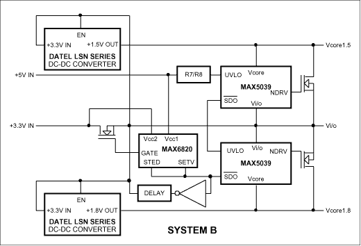
Figure 17. Parallel type-B system.
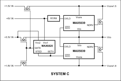
Figure 18. type-c system.
It is recognized that this type of ENABLE output does not fit all regulator / converter ENABLE control signal requirements. Some converters have positive-true ENABLE inputs, while others have positive-true DISABLE inputs. Some, like the Power Trends PT6600 series, require an open-collector current-sinking DISABLE drive while others, like the DATEL LSN series, require a current-sourcing DISABLE drive. Converters built with the MAX1842 controller chip are well served directly by the MAX5039 / SDO \ current sinking / sourcing output.
Table 2 lists the enable / disable requirements of some commercially available modular converters.
Table 2 ENABLE Circuit Requirements
| PRODUCT | ENABLE SIGNAL MUST | DISABLE SIGNAL MUST | MAXIMUM APPLIED VOLTAGE |
| DATEL LSN Series | Open or LOW | Source 3mA @> 2.25V | Converter Input + Voltage |
| Power Trends PT6600 Series | Open or HIGH | Sink 0.5mA @ <0.35V | + 5V |
| MAX1842 | HIGH Source 1µA @> 2.0V | Sink 1µA @ <0.8V | Converter Input + Voltage |
Some practical enable / disable interface circuits that will meet almost any requirement are shown in Figure 19. Optional delayed-ON circuits are included. The third circuit provides a function specifically for Datel LSN series converters where the control input is positive-true DISABLE or negative -true ENABLE. With this converter, the unit is enabled if the input is open or grounded; and the input should not rise above the power input voltage level. As the MAX5039 / MAX5040 / SDO \ output will source current when its output is high , an interface PNP transistor is best used at this interface when the converter is powered from + 3.3V. The circuit is not required when the converter is powered from + 5V. The circuit includes R2 to ensure that the converter DISABLE pin is driven high ( disabled) during a period when the MAX5039 is not powered.
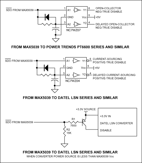
Figure 19. Enable signal interface ciruit options including delayed options.
Larger Image
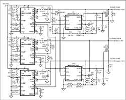
Figure 20. Complete type-A system circuit utilizing MAX1842 step-down controller ICs.
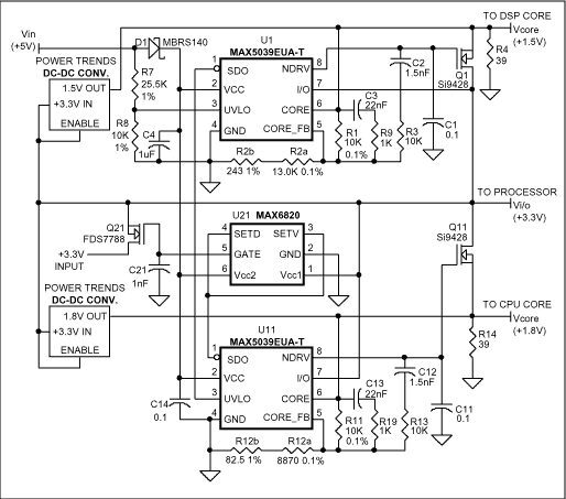
Figure 21. Complete cascade type-B system circuit.
A complete circuit for a parallel type-B dual-tracking system is shown in Figure 22. The + 3.3V output voltage rate of rise is controlled by C21, and the + 1.5V and + 1.8V rate of rise is controlled by the enable characteristics of the converters themselves. This circuit works well with Datel LSN series converters. With this configuration where startup control is by application of VIN (+ 5V), it is important that the 1.5V and 1.8V converter outputs reach final value within 10ms after application of VIN (+ 5V) power.
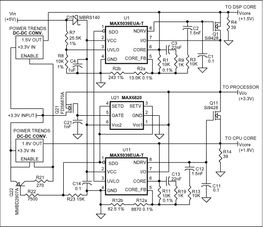
Figure 22. Complete parallel type-B system circuit.
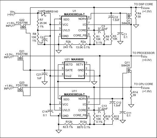
Figure 23. Complete type-C system circuit.
When the supply-voltage sources cannot be individually enabled / disabled the addition of series MOSFET switches and a single MAX6820 (SOT23) voltage sequencer IC satisfies the additional control requirement.
Nearly any power-system voltage tracking requirement can be satisfied directly with one of the completely detailed circuits proposed, or a simple variation thereof, and nearly any enable / disable interface can be properly mechanized with one of the enable interface circuits proposed.
The Component-Selection Spreadsheet simplifies the process of tracking circuit design. Custom EV kits and technical assistance are available when appropriate.
Reference [1] This is accomplished by inserting a Schottky diode in series with the VCC line after the UVLO sensing network as shown in Figures 2 & 3.[2] VREGNOM is the term used in the data sheet; VCT is used here for brevity.
[3] The E96 series is the 100, 102, 105, 107 series; the E24 series is the 100, 110, 120, 130 series. There is also an E192 MIL-STD sequence that is the 100, 101, 102, 104 sequence, but it is uncommon.
[4] The data sheet erroneously suggests a minimum open-loop gain of 200.
[5] If VCT should be selected very close to VREF, say 0.9-1.0V, then one may wish to set R1 <10k
High-power Led Street Lamp is a kind of mainstream light source configuration widely used in Road Lighting project.The aluminum alloy surface of its radiator is treated with deep anodic oxidation, which can resist all kinds of harsh environment.In addition, its patented vertical natural convection heat dissipation structure, high heat dissipation efficiency, small volume, light weight, at the same time, it uses high quality long life LED packaging materials, LED light pass maintenance rate.

Technical parameters
|
Power source |
AC85~260V/50~60Hz |
|
Power |
60W-120W |
|
LED junction temperature |
<60℃ |
|
LED luminous efficiency |
>100 Im/W |
|
The initial light flux |
6000Lm-12000Lm |
|
Light output efficiency of light |
>90% |
|
Color temperature |
4000K-6500K |
|
Color rendering |
Ra>75 |
|
Power factor |
>0.95 |
|
Protection class |
IP65 |
|
Operating temperature |
-40℃~+50℃ |
|
Wind Index |
12 level |
|
Lamp life |
>50000h |
High Power Led Street Lamp,Led Street Lamp,Led Street Lamp Bulbs,Led Street Lamp Price
Jiangsu chengxu Electric Group Co., Ltd , https://www.satislighting.com