Background In the United States, AM/FM radios are still very popular; however, the days of simple car radios are gone, replaced by new car infotainment systems. You no longer have to dial a few knobs and watch an analog display on the way to commute as you have in the past. Today, we can easily grasp the vast amount of information and enjoy the colorful entertainment through the car infotainment system without any effort. Extensive advances in technology and products such as touch screens, digital audio broadcasting (DAB), Bluetooth communications, digital and high definition television (HDTV), satellite radio, integrated cellular phones, CD/DVD/MP3 players, global positioning systems (GPS) Navigation and video game systems, etc., have created a mature entertainment center in the car! This article refers to the address: http:// With new products such as the LTC3589-1 and LTC3589-2 PMIC from Linear Technology, system designers will be able to take advantage of new processors from Freescale, Marvell, Samsung and other companies in their expanding applications. All the energy and performance advantages. The LTC3589 solves many of the traditional issues associated with automotive infotainment system design, improving the driving experience of new cars. We are sure that this is what our fathers hoped to have in their own car and failed to do so ! Composite Post Insulator,also known as Composite Polymer Post Insulators or silicone rubber insulators,which is made of one piece of porcelain but has fixing clamp arrangement are in both top and bottom end. As the replacement of porcelain insulators, Composite Long Rod Post Insulators have many advantages compared to porcelain insulators. Post Insulator are ideal for use in hvac, hvdc and in most hv application.
7.The installation size is the same as porcelain in type, they can exchange to use each other
MAIN DIMENSIONS AND STANDARD PARTICULARS
Type
33KV 10KN Horizonal
33KV-10KN Vertical
Rated Voltage(KV)
33
33
Rated mechanical strength load(KN)
10
10
Creepage distance(mm)
1080
1385
Structure height(mm)
550
708
Insulating distance(mm)
341
526
Lightning impulse withstand voltage(KV)
245
-
1 min wet power frequency withstand voltage(KV)
110
-
Standard
IEC61952
IEC61952
We warmly welcome friends both domestic and abroad to visit our company, if you have any questions, please contact with us directly. Post Insulator,Composite Post Insulator,Composite Long Rod Post Insulators,Composite Polymer Post Insulators FUZHOU SINGREE IMP.& EXP.CO.,LTD. , https://www.cninsulators.com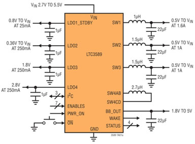
Features
1.Excellent anti-pollution performance, suitable for high polluted area
2.Free of cleaning, economical maintenance and suitable for difficult maintenance area
3.No need of zero value check
4.Light weight, easy and economical to transportation and installation
5.Not brittle, and reduce the purchasing quantities for spare parts
6.Use in HVAC, HVDC and in most HV application.


At the heart of such infotainment systems is a complex microprocessor. Freescale, Intel, ARM and other companies offer a large number of high-efficiency microprocessors, and these growing microprocessors are designed to deliver low-cost wireless, embedded and networking applications. Designed for power consumption and high performance processing. The original intent of these products is to enable original equipment manufacturers (OEMs) to develop portable, handheld devices that are smaller, more cost effective, and have long battery life, while providing enhanced processing performance to run multi-media applications. . Recently, the need for this combination of high efficiency and processing performance has expanded to non-portable applications. Therefore, automotive infotainment systems and other embedded applications also require similar levels of efficiency and processing performance. In all cases, however, in order to properly control and monitor the microprocessor's power system and ensure that all of the processor's performance benefits are realized, a highly dedicated, high-performance power management partner IC will be essential.
The challenges facing automotive PMICs
Electronic system design for automotive applications is challenging because of the wide range of operating temperatures, stringent EMC and transient requirements, and the high quality standards required by automotive OEMs. From the wide operating temperature range, power management ICs face two challenges. The first is power conversion, which must consume a certain amount of power even with high efficiency. When multiple DC-DC and LDO regulators are integrated into a single device, the combined power dissipation can be quite large, easily exceeding 1W. A typical PMIC package such as a 6mm x 6mm 40-pin QFN has a thermal resistance of 40°C/W, resulting in a junction temperature rise of more than 40°C. If the second challenge (ie, wide operating ambient temperature) is taken into account, then the maximum junction temperature of the PMIC often exceeds 125 °C. Even in body electronics (and not under the hood), the ambient temperature inside the sealed plastic electronic control module is likely to reach 95 °C. Due to these temperature challenges, many PMICs that are rated for 85°C or even 125°C temperature conditions are not sufficient for continuous operation in high temperature environments.
Another important thing to operate an integrated power management device under high ambient temperature conditions is that the device must monitor its own internal chip temperature and report when the junction temperature is about to reach an excessive level so that the system can How to reduce the power supply of the load makes smart and flexible decisions. System software can achieve this by turning off less critical functional circuits or reducing the performance of processors and other high-power functional circuits such as displays and network communications.
Today, the interior of the car's dashboard is packed with a variety of electronic circuits and components. Moreover, it is likely to be plugged into wireless communication functions such as Bluetooth to cellular phone-based network connections. Therefore, if new components are to be installed in an environment where heat dissipation conditions are severely limited, it is important that these new components do not generate excessive heat or EMI. The electromagnetic compatibility (EMC) requirements here are very strict, involving radiation and conducted emissions, radiation and conductive resistance or sensitivity, and electrostatic discharge (ESD). To have the ability to meet all of these requirements, many of the performance aspects of PMIC design will be affected. Some of these effects are straightforward. For example, a DC-DC switching regulator must operate at a fixed frequency well beyond the AM radio band. However, another common source of radiated emissions in DC-DC converters comes from the switching edge rate of their internal power FETs.
Many of today's embedded systems and advanced processors require controlled and well-designed sequencing when power is applied and applied to a variety of different circuits. Providing system flexibility and simple sequencing methods not only simplifies system design, but also ensures system reliability and allows a single PMIC to handle more systems, not just to meet a specific processor requirement.
To sum up, the main challenges faced by automotive infotainment system designers include:
· Tradeoff between power dissipation and high integration of multiple switching regulators and LDOs
· Monitor junction temperature
· Radiation emission and conduction emission resistance
· Large voltage transients and extreme temperatures
· Manage power sequencing
· Minimize solution size and footprint
a simple solution
Historically, many existing PMICs do not yet have the necessary power to handle these new systems and microprocessors. For any solution designed to meet the above automotive power management IC design constraints, it must be highly integrated (including high current switching regulators and LDOs), wide operating temperature range, power sequencing, and dynamic key parameters. I 2 C control and "hard to implement" functional components (eg buck-boost regulator). In addition, devices with high switching frequencies can reduce the size of external components, while ceramic capacitors reduce output ripple. Although the input voltage is typically taken from a pre-conditioned system or battery voltage, such ICs must also have the ability to adapt to harsh automotive environments, including radiation emission suppression.
A high power PMIC for today's infotainment systems
The LTC®3589-1 and LTC3589-2 are complete power management solutions for ARM-based processors and advanced portable microprocessor systems. These devices include three synchronous buck DC/DC converters for core, memory and SoC rails, one synchronous buck-boost regulator for I/O, and three for low noise Analog power supply 250mA LDO regulator (see Figure 1). An I2C serial port is used to control regulator enable, output voltage level, dynamic voltage regulation and slew rate, operating mode, and status reporting. The voltage regulator initiated sequencing operation is accomplished by connecting its output to the enable pin or through the I2C port in the desired order. System power-up, power-down, and reset functions are controlled by button interface, pin input, or I2C interface. The voltage monitor and active discharge circuit ensure a clean power-down before the next enable sequence, and the selected regulator eliminates button control for the power supply (for example, memory when it must be in standby mode Keep it running). The LTC3589 supports i.MX, PXA, and OMAP processors with eight independent power rails, proper power values, and dynamic control and sequencing. Other features include interface signals such as the VSTB pin, which switches between set operating and standby output voltages on up to four power rails simultaneously. The device is available in a low profile 40-pin 6mm x 6mm bare pad QFN package.
Figure 1 : Simplified block diagram of the LTC3589
The LTC3589 solves the above-mentioned automotive infotainment system design challenges. The LTC3589HUJ PMIC offers a high temperature (Class H) device option with a junction temperature range of -40°C to +150°C, which easily meets the high temperature operating requirements of automotive applications. The IC includes a thermal alarm flag and interrupt output specifically for junction temperature monitoring, as well as a thermal shutdown protection that provides reliable hardware protection in the event of improper power dissipation or severe failure.
The LTC3589 PWM switching frequency is specially trimmed to 2.25MHz (which guarantees a range between 1.8MHz and 2.6MHz). Alternatively, the regulator can be set to a forced continuous PWM mode of operation to prevent pulse skipping or burst mode (Burst Mode® operation, even at light loads. This not only keeps the frequency fixed, but also It also reduces the voltage ripple on the DC-DC output capacitor.)
Inhibition of radiation and conducted emissions
The LTC3589 has a special feature that allows the user to slow down the switch edge rate specifically to reduce radiation. This can help optimize power converter efficiency by selecting the appropriate edge rate to achieve "both meets emission standards while minimizing switching losses." This edge rate control is available on all three buck switching regulators in the LTC3589.
In addition, there are four switching regulators and related reactive devices built into the IC that need attention. One possible approach is to shield the area where the LTC3589 is located to prevent EMI emissions. In addition to being expensive and cumbersome, this method has not solved the contamination problem caused by any wires that may be connected to the power supply area. A better approach is to suppress the source of radiation and eliminate the antenna.
Radiation source suppression avoids the generation of RF energy by using reasonable layout/component selection. Shielded inductors must be used and these inductors should be placed farther than the output capacitor LTC3589. This is because the AC current circulates along the route of LTC3589 → Inductor → Output Capacitor → Ground → Return to LTC3589. It is also apparent that a wide trace (preferably a region fill) should be used to connect the ground of the output capacitor to the ground of the LTC3589 and to the ground of the PVIN input decoupling capacitor.
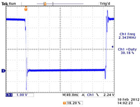
The LTC3589 also offers several methods for radiation source suppression. The switching slew rate on the buck regulator can be adjusted from 1 ns to 8 ns with I 2 C. Since these buck regulators are synchronous, both rise and fall times are under control. Figure 2 shows the switching operation graph for the rise and fall times of 1 ns.
Figure 2 : Buck Regulator Switch Operation ( with 1ns rise and fall times )
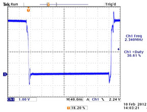
Figure 3 shows the switching operation graph with 8ns rise and fall times. As can be seen from the figure, when the conversion time is 8 ns, the ringing during the conversion operation is greatly reduced.
Figure 3 : Buck Regulator Switch Operation ( with 8ns rise and fall times )
In addition to switching time control, the LTC3589 offers several other EMI suppression methods. The frequency of the buck regulator can vary from 2.25MHz to 1.125MHz. Moreover, to minimize input ripple (which is ultimately radiated through the power input wiring), the buck regulator can be interleaved between two different phase clocks.
The LTC3589 can deliver significant power in excess of 10W. This results in a considerable circulating current and therefore an uninterrupted path must be provided for this current cycle. In particular, a gap in the ground plane that causes a large circulating current to flow around it, resulting in a slot antenna. However, other obstacles such as layer changes provide some energy to the EMI signature signal and should be minimized. Ideally, the top and bottom layers should be all (or most) ground planes and the signal layers inside. This is often impractical, so some design ideas will naturally focus on how to connect the ground plane before the layout begins. For example , it is not a good idea to place the LTC3589 on a corner or bump on the PCB . This will make the proper routing of the ground plane very difficult. Moreover, it is appropriate to first route the high circulating current region of the LTC3589 to ensure the best possible layout.
If EMI control can be planned and implemented with radiation source suppression and antenna cancellation, a full power system with excellent EMI performance can be created without increasing product cost or weight.
Other important features
The LTC3589 is fully compliant with automotive ESD requirements for 4kV HBM, 200V MM and 1.5kV CDM, another key requirement for approaching zero defects in automotive assembly. In addition, the IC has a very low standby current consumption (typically 9μA), a feature that meets the requirements of car navigation, theft prevention, and security systems that must maintain continuous power to the real-time clock circuitry for sensing time.
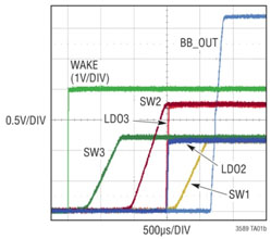
Finally, the LTC3589 supports simple and efficient power sequencing, which can be handled by serial communication or pin-bonding (connecting the power supply output voltage to the enable pin in the desired order). A delay of 200 μs was internally made for each enable action to further stagger the time of the start sequence. This feature is supported by a precision low voltage enable threshold, so sequencing can be done with supply voltages as low as 0.55V. In addition, a soft start is applied to each supply voltage output to limit inrush current and achieve a clean voltage transition. Each regulator output includes an internal pull-down resistor that goes into operation when the regulator output is deactivated to ensure controlled discharge and a low starting point for the next turn-on sequence. See Figure 4.
Figure 4 : LTC3589 Startup Sequence
in conclusion
Today's cars have made great strides compared to their former drivers. Simple AM/FM radios have given way to the latest technological advances such as satellite radios, touch screens, navigation systems, Bluetooth, HDTV, integrated cellular phones, media players and video game systems. Moreover, by replacing discrete power IC components or over-integrated traditional large PMICs (ie with audio, codecs, etc.), system designers will be able to adopt a new generation of compact PMICs that integrate critical power supplies Management capabilities designed to achieve new levels of performance with smaller and simpler solutions. High-performance mobile processors typically have a unique set of power requirements, including multiple high-current and low-noise voltage rails, programmable sequencing, and dynamic I 2 C regulation. These high-end processors were originally developed for handheld applications, but are now being deployed in non-portable and embedded systems such as automotive infotainment systems.