Abstract: This paper introduces the main performance characteristics and basic working principles of the class A-B audio power amplifier NCP2890 of ON Semiconductor, and gives the typical application circuit and design method of designing audio power amplifier with NCP2890. 1 Overview NCP 2890 is the first audio power amplifier in the cost-effective, full-featured audio series launched by ON Semiconductor. It is designed and produced for battery-powered wireless devices such as mobile phones and PDAs. A very good quality wireless application class A-B audio power amplifier can provide customers with excellent audio performance. The device has outstanding power supply rejection ratio (PSRR) and total harmonic distortion plus noise (THD + N) characteristics, while integrating external control gain characteristics and adjustable power-on and power-off delay functions, and has "power-on and power-off" control The circuit can eliminate the audible noise generated when turning on and off such audio power amplifiers, and can be flexibly applied to the design of portable audio equipment. NCP 2890 allows lithium ion or lithium polymer batteries to be powered directly, thereby eliminating the need for an additional low-dropout regulator (LDO), while reducing the board footprint and overall cost. In order to meet the needs of specific markets, NCP 2890 currently has two different package forms of Mi-crobump-9 (2.25mm2) and Micro-8 (14.7mm2). Figure 1 shows its pin arrangement, each pin The functions are listed in Table 1. NCP2890 includes 671 transistors and 1899 MOS gates, so it has excellent audio performance. Table 2 shows the main performance parameters of NCP2890. 3 Application circuit design Figure 2 shows the typical application circuit of NCP2890 audio power amplifier. From Figure 2, it can be seen that there are only a few components around the NCP2890 for adjusting the gain, an input coupling capacitor, a bypass capacitor, etc. It's extremely simple. 3.1 The working principle of the circuit NCP 2890 contains two identical power amplifiers, the input audio signal is output from OUTA after being amplified by the first power amplifier. The voltage gain is determined by the ratio of the external resistor Rf and Rin. The amplified audio signal is inversely amplified by a second power amplifier with a gain of 1 and output from OUTB. Because the audio power signals output by OUTA and OUTB are equal in size and opposite in phase, and the DC static potentials of both outputs (OUTA and OUTB) are the same (Vp / 2), the speaker can be directly connected to OUTA and OUTB. There is no need to increase the output coupling circuit. The output stages of the two power amplifiers are specially designed using PMOS and NMOS transistors. During normal conduction, its channel resistance is less than 0.6Ω, so its output waveform distortion is very small. General power amplifiers will produce audible noise in the human ear during the turn-on and turn-off process. In order to eliminate this audible noise, a noise canceling circuit has been specially designed inside NCP 2890. At startup, a logic high level is added to the switch control terminal, and the DC voltage value on the bypass capacitor Cby begins to increase exponentially. When the voltage value reaches the common mode voltage value (Vp / 2), the output power starts (this process is about 50ms); while the shutdown, the control terminal is connected to a low level, the load is connected to the ground terminal, the output power is zero, and the DC static current of the circuit is less than 100nA. 3.2 Circuit element parameter setting Rin and Rf are used to set the closed-loop gain of the amplifier. In order to optimize the performance of NCP 2890, the closed-loop gain of the amplifier should be set at a lower level. At this time, the THD is the smallest, the signal-to-noise ratio is the largest, and the frequency response range is the widest. Therefore, in most cases, the amplifier's closed-loop gain is generally set between 2 and 5. Therefore, the value of the input resistance (Rin) D is more suitable at 20kΩ, and Rf is used to adjust the closed-loop gain to control the output power. The input coupling capacitor Cin is used to isolate the DC voltage at the input of the amplifier, and can form a high-pass filter with Rin, but it will affect the lower cut-off frequency of the filter. In order to prevent the low-frequency signal from decaying too much, in theory, Cin should take a larger value, and the charging and discharging time of the larger-capacity capacitor is longer, so it takes a longer time to make the static potential of the input terminal reach Vp / 2 , And it is easy to cause startup noise at the output. Therefore, in most cases, the value of Cin is generally between 0.1 and 0.39μF (Rin = 20kΩ). The bypass capacitor Cby is a common-mode voltage (Vp / 2) filter, which is a key component that determines the length of the startup time and reduces the startup noise. In most cases, the bypass capacitor Cby is preferably 1.0μF. 3.3 Precautions for use When the circuit reaches the maximum output power? Poms = 1.0W, Vp = 5.0V, RL = 8.0Ω ?, the peak current on the load is 500mA. In order to prevent excessive output current when the output load is disconnected, an output current detection circuit is provided in the chip, which can limit the maximum output circuit to 800 mA. In this way, once the output current exceeds 800mA, the four MOS transistors at the output will be turned off by the gate voltage and no longer output current. When the chip temperature exceeds 160 ℃, the internal amplifier will be shut down and stop working, until the temperature is lower than 140 ℃, the internal amplifier will restart to work. Although NCP 2890 contains over-current and over-heat protection circuits, when using it, it must be noted that the power supply voltage cannot exceed its limit value to avoid damage to the chip. Follow WeChat Download Audiophile APP Follow the audiophile class related suggestion Fairchild Semiconductor has developed the FAB1200 stereo Class-G ground-referenced headphone amplifier with integrated buck converter, and with ... NS4248 is an ultra-low EMI, no filter, 3W dual channel Class D / AB chip-selected audio power amplifier + stereo headphone amplifier ... High-quality audio power amplification Output 50W audio power amplifier circuit diagram Chapter One Common Principles and Applications of Electronic Components Lecture 1: Resistors and Ohm's Law Working principle and application of 555 time-based integrated circuit & nb ... Chip inductors are also known as surface-mount inductors, and they are combined with other chip components (SMC and S ... 2002, Issue 6, Category: Electronic Products and Devices ... Abstract: Based on the Meteor II Standard image acquisition card, to identify the Data Matri ... Abstract: HA7279A is an intelligent keyboard and LED special control chip, which has a serial interface and can simultaneously drive 8 common negative digital ... '+ data.data.username +' '; dom + =' 1080P Home Projector-1080P high-definition picture presentation, immersive experience, leisure and entertainment, enjoy games, videos, TV series, photos, sports, UEFA Champions League, etc. Mini Portable Projector, small and light, to carry and use, environmentally friendly micro LED flat light source design extremely long life 1080P Home Projector,Home Cinema Projectors,Projector For Room,1080p hd projector,1080p home cinema projector Shenzhen Happybate Trading Co.,LTD , https://www.szhappybateprojectors.com
2 Chip structure and performance parameters Microbump -9 Micro8 Name Features A1 4 INM Audio signal inverse input, external Rf and Rin A2 5 OUTA Inverting output, external load A3 3 INP Non-inverting input B1 NA VM_P Ground B2 7 VM Ground B3 6 Vp Power input terminal, the voltage range is 2.2V-5.5V C1 2 BYPASS External bypass capacitor terminal C2 8 OUTB In-phase output, external load C3 1 SHUTDOWN Shutdown control terminal, active low
Table 2 NC2890 main performance parameters Parameter The smallest Standard The largest Unit Power supply voltage (Vp) 2.6 5.5 V Output power (Po) 0.28 1.08 W Efficiency (η) 63 % Quiescent current (Idd) 1.5 1.7 4.0 mA Total higher harmonics plus noise (THD + N) 0.02 % Power supply rejection ratio (PSRR V +) -74 dB Signal to noise ratio (SNR) 84 dB Starting voltage V (SDIH) 1.2 V Shutdown voltage (VSDIL) 0.4 V Startup time (TWU) 285 ms Closing time (TSD) 385 ms 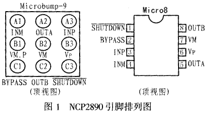
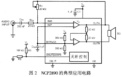
The voltage dividing circuit composed of R1 and R2 is used to generate the starting voltage of the chip. Generally, R1 takes the value of 100kΩ. The resistance value of R2 can be selected according to the voltage value during design, as long as the voltage dividing value is greater than about 1.2V. 


'+ data.username +'
'+ data.username +'
'; dom + ='
'; $ (' # follow_list '). append (follow_user);} if (data.status == "failed") {alert (data.msg);}});} else {// Unfollow if ($ ( this) .attr ('id') == 'cancelFollow') {$ .post ('/ d / user / cancelFollow', {tuid: article_user_id}, function (data) {// Data format returned: if (data .status == "successed") {follow_wrap.html ('Follow'). attr ('id', 'follow'). css ('background', '# f90'); $ (". followNum strong"). html (-getFollowNum); $ ('# follow_list .face'). each (function () {var target_uid = $ (this) .attr ('data-uid'); if (target_uid == now_uid) {$ ( this) .remove ();}})} if (data.status == "failed") {alert (data.msg);}}); return false;}}});});}); / * var myface = "{$ _super ['uid'] | avatar}"; var myname = "{$ _super ['username']}"; var article_id = {$ article ['id']}; var article_user_id = {$ article ['mid']}; // Article author ID $ (function () {<notempty name = "clearnum"> // Reduce the number of reminders var count = parseInt ($ ("# noticeCount"). html ()); count = count-{$ clearnum}; $ ("# noticeCount"). html (count); if ( count
Interesting and informative information and technical dry goods
Create your own personal electronic circle
Lock the latest course activities and technical live broadcast
comment
Publish
Fairchild's audio amplifier can effectively balance audio power and battery life
Posted on 2011-07-22 09:18 • 302 times read
Nanochip Technology launches Class D / AB Class Chip Audio Power Amplifier NS ...
Published on 2010-08-12 09:00 • 712 views
High-quality audio power amplification
Posted at 2009-05-08 13:44 • 208 times read
Output 50W audio power amplifier circuit diagram
Published on 2008-12-17 14:29 • 491 times read
Principles and applications of common electronic components
Posted at 2006-04-16 23:47 • 2018 times read
Working principle and application of 555 time base integrated circuit
Published on 2006-04-16 23:34 • 1570 views
Principle and application of chip inductance
Posted at 2006-04-16 23:32 • 388 views
[Photo] The principle and application of RF receiving integrated circuit GY2800
Published on 2006-04-15 19:21 • 515 views
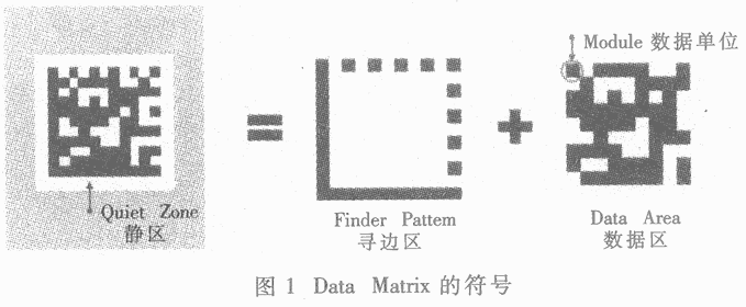
Data Matrix QR code image processing and ...
Published on 2006-03-24 13:30 • 1065 times read
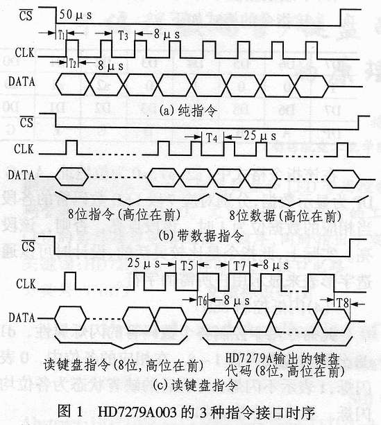
Programmable digital tube / keyboard serial interface chip HD7279A original ...
Published on 2006-03-24 12:58 • 469 views