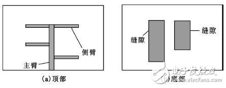
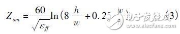
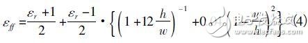
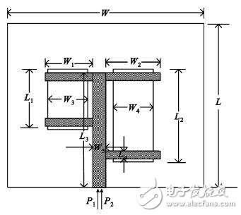
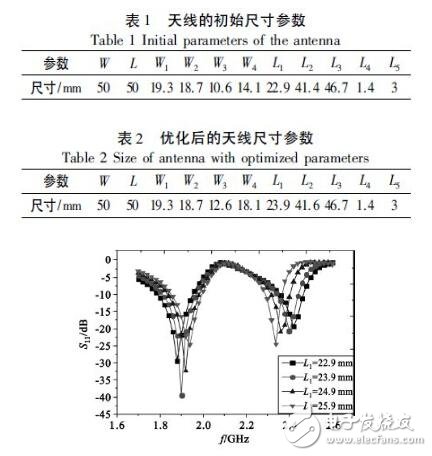
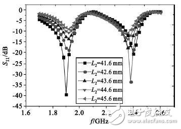
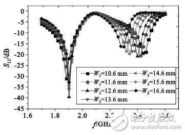
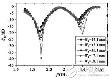
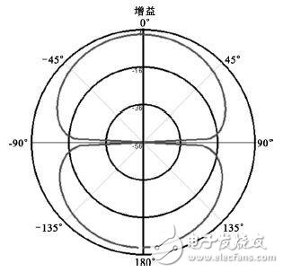
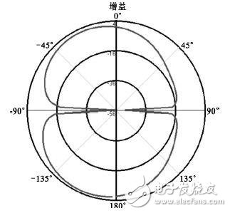
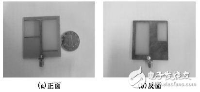
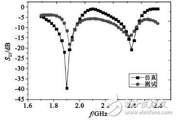
With the rapid development and maturity of the Internet of Things technology, ultra-low power wireless sensors have become an important component of the Internet of Things. Wireless sensor networks deploy a large number of sensor nodes in the monitoring area and use radio communication to form a multi-hop self-organizing network system with dynamic topology, which has been widely used. However, if the sensor node with the traditional power supply mode runs out of battery, it needs to replace the battery. If there are a large number of sensor nodes, the work required to replace the battery manually will not be neglected. With the increasingly mature ultra-low-power chip technology, collecting radio frequency energy in the surrounding environment to provide electrical energy has become an effective and feasible new energy supply model. In recent years, with the rapid development of communication technologies, the environment is flooded with a large number of radio wave signals, mainly including the mobile phone (GSM) band and the industrial communication (ISM) band. For a long period of time in the future, multiple communication networks coexist, and it also provides abundant radio frequency resources for RF energy collection systems. The most important part of the wireless energy acquisition technology is the analysis and design of the receiving antenna, and it is also a hot spot concerned by experts and scholars at home and abroad. Microstrip antennas have many advantages such as low cost, light weight, and easy conformity, and are widely used in various communication systems. However, since the microstrip antenna has a narrow frequency band and limits its practical application, adding a parasitic element or a rectangular patch element having a different shape gap can overcome the narrow-band characteristics of the microstrip antenna; at present, at a high frequency band, the slot antenna at home and abroad A lot of research reports have been conducted. The slot antenna structure of the basic structure has good performance, but there are also inherent defects such as narrow impedance bandwidth and single frequency operation. Therefore, multi-frequency/broadband technology has become a hot topic in the research of slot antennas. The "Design of a 2.4GHz/5.2GHz Dual-Band Microstrip Slot Antenna" on the basis of the slot antenna reloads two inverted u-grooves to achieve dual-frequency operation at 2.4/5.2 GHz; The design of a miniaturized dual-frequency slot microstrip antenna "opens an F-type slot in the ground plane and feeds it with a microstrip line. The main dimension of the slot is used to operate the antenna in the 2.4 / 5.8 GHz band. The "Design of a Bandwidth Circular Slot Antenna" uses a fork type microstrip line to feed and opens a circular slot antenna on the ground plate by adjusting the relative positions of the microstrip line terminal and the center of the slot and the radius of the circular slot. To get the best match, the frequency band reaches 32.5% when the antenna is operating at 2 GHz. However, due to the low signal power spectral density in the surrounding environment in the 5 GHz frequency band, these antenna designs are not suitable for environmental wireless energy collection. Through the analysis and research of the above documents, a small dual-frequency microstrip feeding slot antenna suitable for wireless energy collection is proposed in the paper. The antenna is based on a fork-type microstrip feed slot structure and adopts reactance loading method, ie, by loading microstrip stubs and slots to achieve dual-band operating characteristics, to increase the operating bandwidth of the antenna, and to overcome the narrow-slot microstrip antenna while ensuring performance. Bandwidth defects. Through the simulation analysis, the general law of the working frequency of the slot antenna changes with the gap size. Based on the microstrip antenna structure, the dual-frequency operation can be realized by using the reactance loading method. At this time, the dual-frequency ratio can be adjusted to be closer. According to the cavity model theory, the input impedance Zin of the microstrip antenna of the thin substrate near the resonant frequency of the mode can be equivalent to In the formula, Xr is the "resonance" reactance of the parallel resonant equivalent circuit of this mode, and Xf is the synthesizing effect of other modes. The characteristic equation of its resonant frequency is Xr + Xf = 0. If a reactance XL is used to load the microstrip antenna, the above characteristic equation becomes Adjust the value of XL, you can get two zeros to achieve dual-frequency work. Figure 1 shows the improved antenna structure. The top of the antenna is a left-right asymmetrical branched microstrip line. The advantage of the branch feed is that this feed method can achieve a wider bandwidth and make the antenna achieve a good impedance match over a wide frequency range. In this design, two rectangular slots are opened in the ground plate, and the best match is obtained by adjusting the relative positions of the branch and slot of the microstrip line and the size of the rectangular slot. Figure 1 The geometric model of the antenna In order to realize impedance matching of the interface, the characteristic impedance of the main arm of the branch microstrip line is 50Ω, and the characteristic impedance of the side arm is 100Ω. The width of the microstrip line can be calculated based on empirical formulae (3) and (4). The equivalent dielectric constant is From this, the corresponding width of the 50Ω microstrip feeder is 3.0 mm, and the width of the 100Ω microstrip line is 1.4 mm. Two rectangular slots are etched on the bottom ground plate of the antenna. This corresponds to the introduction of two reactive elements. Two resonance points are generated. The antenna uses an FR-4 as a dielectric substrate, with a substrate thickness of 1.6 mm, a relative dielectric constant of 4.2, and a loss tangent of TanD = 0.0003. The size of the ground plate is 50 mm & TImes; 50 mm. Because of the presence of edges on the surface of the gap Strong diffracted fields, so choose a suitable media substrate size, you can get a better far-field pattern. The feed point is in the center of the broadside and p1 and p2 are differential input ports. In order to further explore the effects of various geometric parameters of the antenna on the return loss of the antenna, the operating characteristics of the GSM 1900 MHz and ISM 2.4 GHz bands are obtained. The ADS full-wave electromagnetic field simulation tool is used to analyze and optimize the parameters of the antenna. The physical parameters of the antenna are shown in Figure 2. Through preliminary simulations, the return loss of the antenna is sensitive to the changes of the lengths L1, L2 and widths W3, W4 of the two rectangular gaps, so the above four parameters are selected for their parameter analysis. Each parameter selects an initial value. When one parameter changes, the other parameters remain unchanged. The initial value of each parameter is shown in Table 1. Figure 2 shows the design parameters of the slot antenna Figure 3 shows the effect of the small gap length L1 on the return loss of the antenna. The L1 dimension is chosen to increase by 1 mm from 22.9 mm. The other main parameters remain unchanged. The simulation results show that the larger the L1 is, the higher the resonance point is in the low frequency range. When L1 = 23.9 mm, the return loss is the minimum; at the high frequency range, as L1 increases, the resonant frequency point shifts to the left, and the return loss decreases but the bandwidth also decreases. Figure 4 shows the effect of large gap length L2 on the return loss of the antenna. L2 increases from 11.6 mm to 1 mm, and all other parameters remain unchanged. It can be seen from the figure that the smaller the L2 at the low frequency band, the greater the return loss and the corresponding increase in bandwidth. The resonance point remains basically unchanged; at higher frequencies, the larger the L2, the resonance point moves to the left, and the smaller the return loss, the more and more the antenna impedance does not match. Figure 5 shows the effect of small gap width W3 on the return loss of the antenna. The size of W3 increases from 10.6 mm to 1 mm, and all other parameters remain unchanged. The simulation results show that W3 has little effect on the low frequency band; when W3 increases at high frequency, the resonant frequency shifts to the left, and the return loss and bandwidth remain unchanged. Figure 6 shows the effect of large gap width W4 on the return loss of the antenna. W4 increases from 14.1 mm to 1 mm, and all other parameters remain unchanged. It can be seen from the figure that the larger W4 is at the low frequency band, the resonant frequency shifts slightly to the right, the return loss increases, and the better the matching of the antenna, the corresponding increase in bandwidth. The pattern at the high frequency band is the same as the low frequency band. Through simulation results, it was found that adjusting the size of the gap can change the distance between the two resonant frequencies. Then based on the design requirements for the band, the size of the final selected slot size is L1 = 23.9 mm, L2 = 41.6 mm, W3 = 12.6 mm, and W4 = 18.1 mm. Finally, the best antenna size parameters are obtained, such as Table 2 shows. Figure 3 Resonant frequency changes with L1 Figure 4 Resonant frequency changes with L2 Figure 5 Resonant frequency changes with W3 Figure 6 Resonant frequency changes with W4 The gain patterns of the antenna at two resonant frequencies of 1.9 GHz and 2.4 GHz are shown in Figure 7 and Figure 8. It can be seen from the figure that the radiation of this slot antenna is bidirectional, and the radiation field above and below the slot is the strongest and the radiation intensity is basically the same. When the resonant frequency of the antenna is 1.9 GHz, the maximum gain on the XOZ plane is 1.4 dBi; when the antenna resonant frequency is 2.4 GHz, the maximum gain on the XOZ plane is 2.9 dBi. The antenna pattern has a certain directionality, but the antenna The gain is not so high, so this antenna can be used as an omni-directional antenna and is suitable for receiving surrounding radio frequency wireless energy. Figure 7 Antenna gain on the XOZ plane (f = 1.9 GHz) Figure 8 Antenna gain on the XOZ plane (f = 2.4 GHz) Based on the parameter analysis and optimization results from the previous section, the antenna was fabricated using an FR4 double-sided PCB board, and the antenna was tested with an Agilent vector network analyzer. The physical image of the antenna is shown in Figure 9. Figure 9 front and back of the antenna Figure 10 shows the simulation of the input return loss of the antenna and the measured curves. It can be seen from the simulation that the center resonance point of the antenna is f1 = 1.9 GHz and f2 = 2.4 GHz. When the return loss S11 is _ - 10 dB At the time, the operating frequency range of the antenna is 1.82~ 1.96 GHz in the low frequency range, the bandwidth reaches 140 MHz, the frequency range of the antenna is 2.34 ~ 2.45 GHz in the high frequency range, the bandwidth is close to 110 MHz. The return loss of the antenna at the resonance point is -40 dB and -20 dB, respectively, indicating that the antenna is well matched. The measured results are basically the same as the simulation results. The resonance frequency band at the low frequency band shifts to the right by about 1.92 GHz. The resonance point at the high frequency shifts slightly to the left, and the return loss at both resonance points is reduced. Causes of errors include minor errors in the dimensions of the antenna during processing, poor soldering at the SMA connector, energy loss at the interface, and environmental interference. Figure 10 Return Loss Test Results In this paper, a multi-band antenna method based on slot loading combined with two-wire feeding is proposed. A novel small size dual-band microstrip slot antenna suitable for environmental wireless energy reception is designed. It was simulated and optimized by Agilent's ADS, and the antenna was operated at dual frequency of 1.9 GHz and 2.4 GHz respectively. The low-frequency bandwidth is 140 MHz, the relative bandwidth is about 7.4%, the high-frequency bandwidth is 110 MHz, and the relative bandwidth is about 4.6%. The RF energy receiving antenna can adapt to both GSM and ISM frequency bands, and the size is small, and the production cost is low. , With strong practicality and good application prospects.
ZGAR PCC KIT
ZGAR electronic cigarette uses high-tech R&D, food grade disposable pod device and high-quality raw material. All package designs are Original IP. Our designer team is from Hong Kong. We have very high requirements for product quality, flavors taste and packaging design. The E-liquid is imported, materials are food grade, and assembly plant is medical-grade dust-free workshops.
From production to packaging, the whole system of tracking, efficient and orderly process, achieving daily efficient output. We pay attention to the details of each process control. The first class dust-free production workshop has passed the GMP food and drug production standard certification, ensuring quality and safety. We choose the products with a traceability system, which can not only effectively track and trace all kinds of data, but also ensure good product quality.
We offer best price, high quality Vape Device, E-Cigarette Vape Pen, Disposable Device Vape,Vape Pen Atomizer, Electronic cigarette to all over the world.
Much Better Vaping Experience!
E-Cigarette Vape Pen,Disposable Device Vape,PCC SET, Vape Pen Atomizer,Latest Disposable E-Cigarette OEM vape pen,OEM electronic cigarette ZGAR INTERNATIONAL(HK)CO., LIMITED , https://www.szdisposable-vape.com