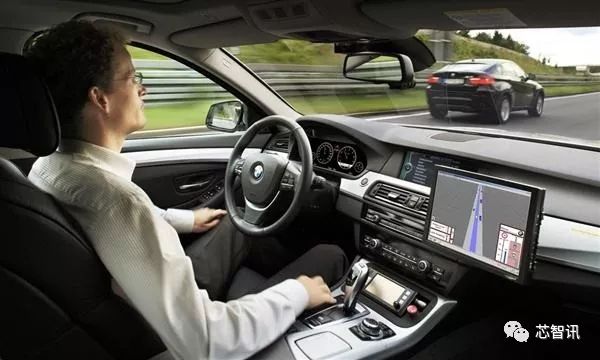
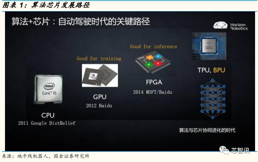
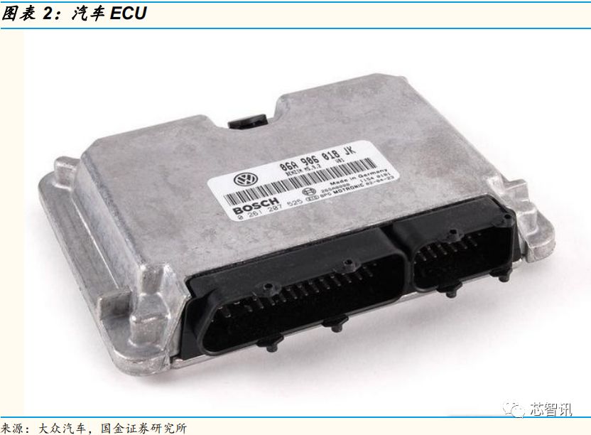
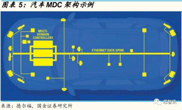
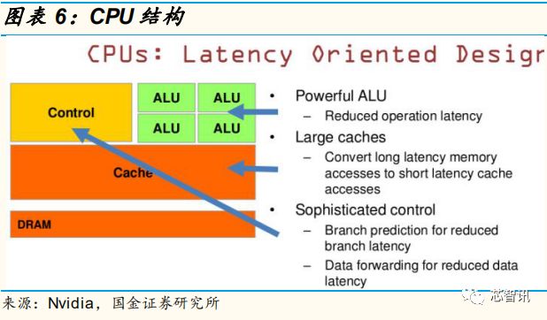
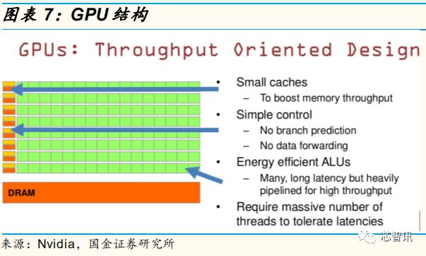
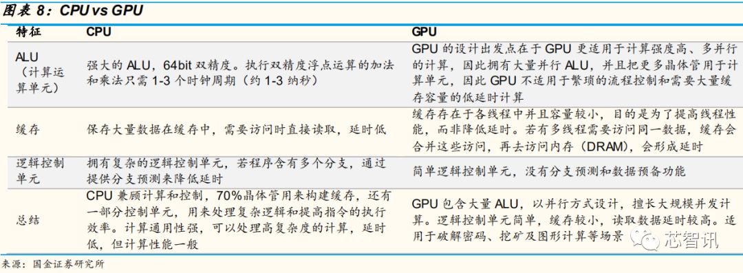
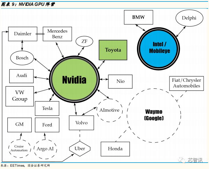
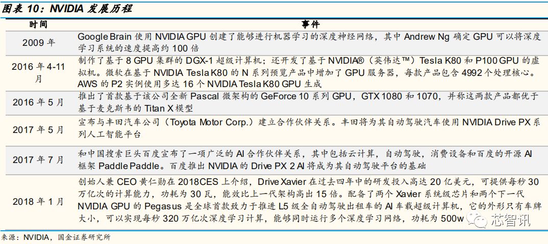
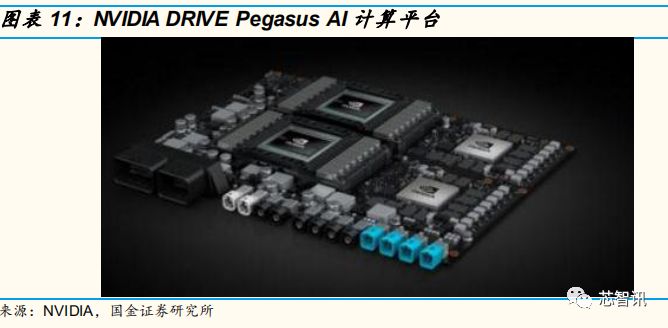
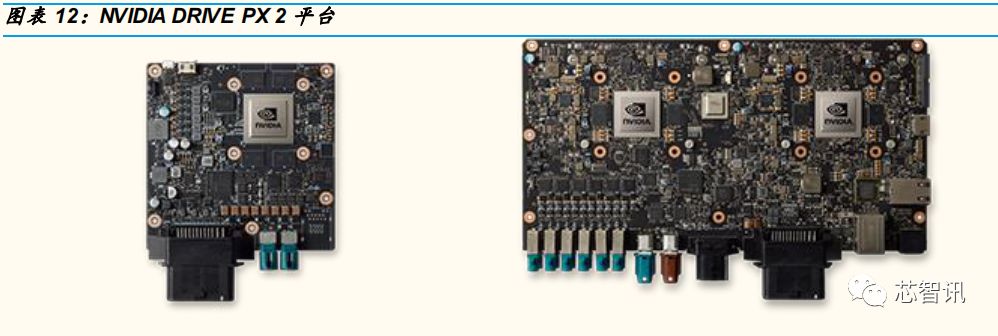
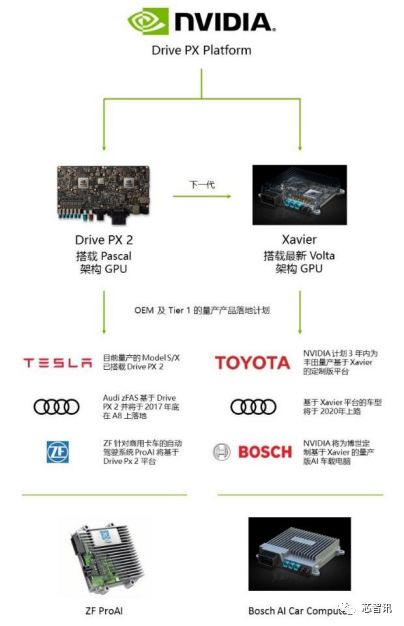
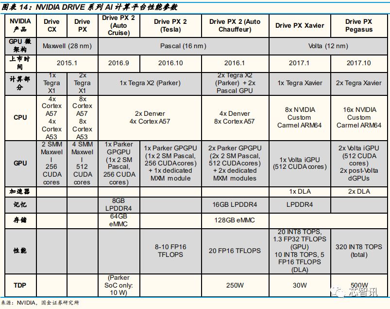
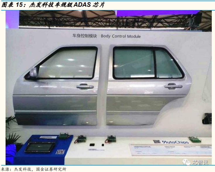
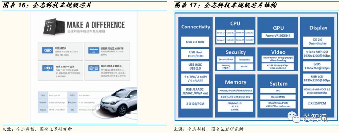
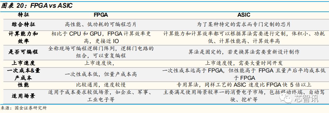
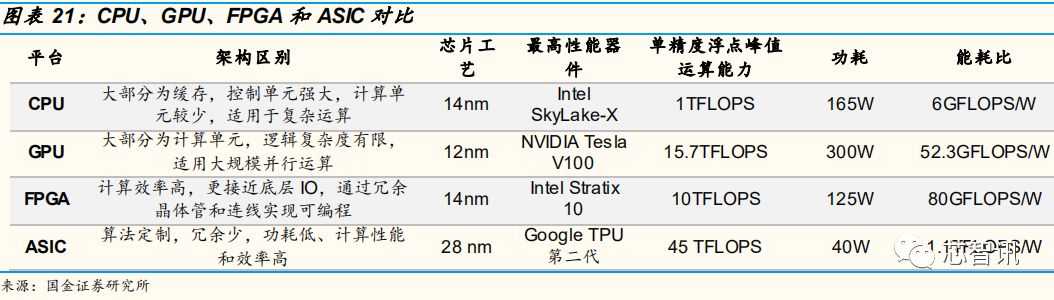
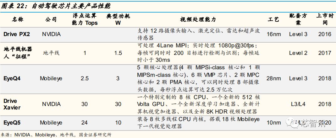
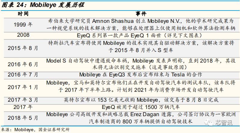
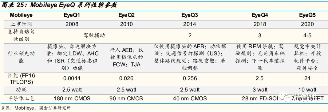
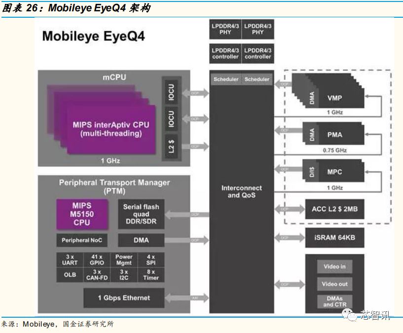
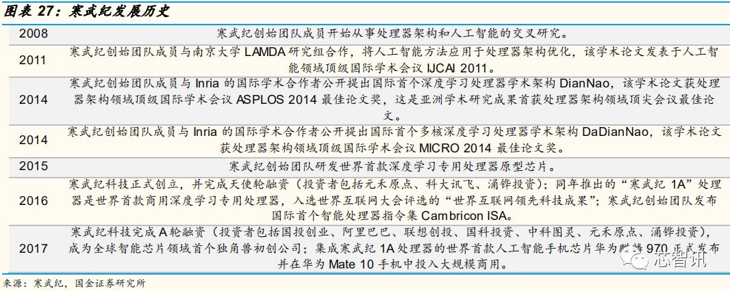
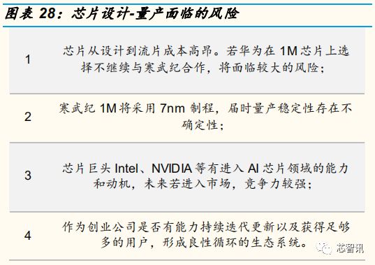
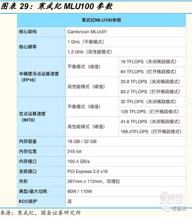
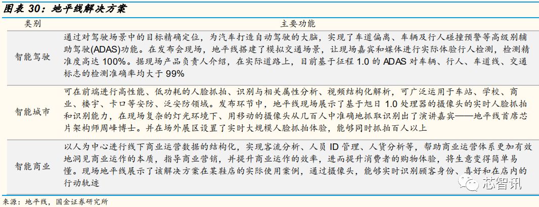
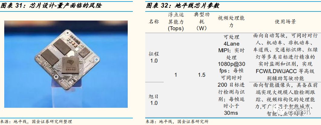
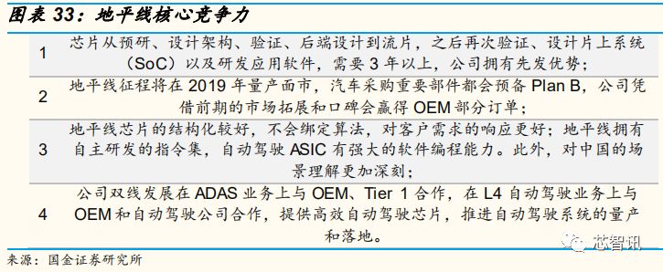
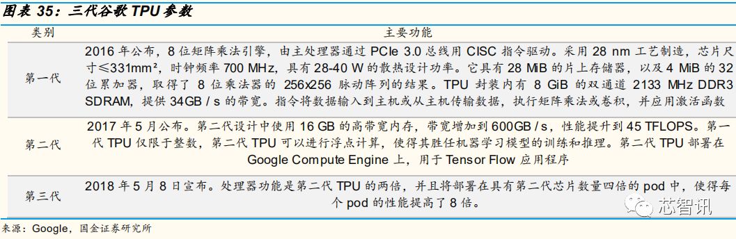
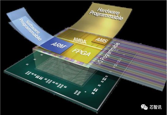
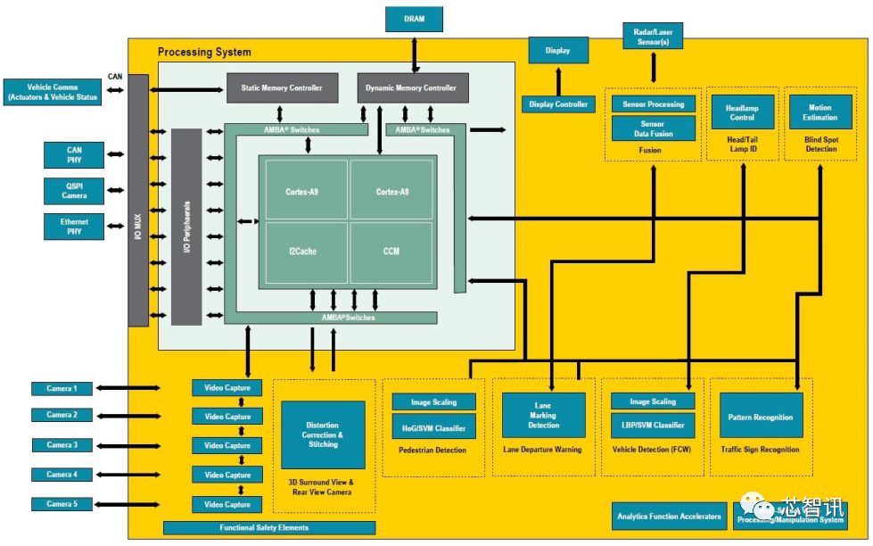
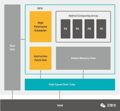
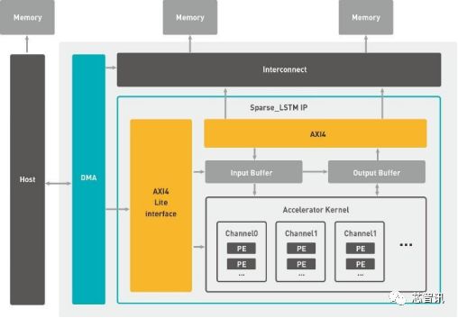
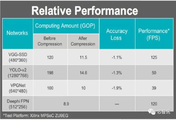
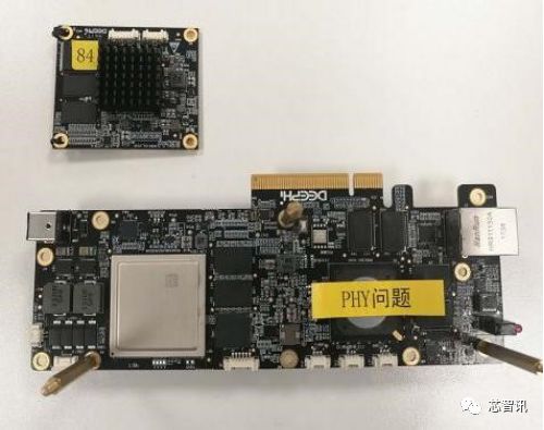
Industry view: In the early stage of automotive electronics development, the distributed ECU architecture was the mainstream, and chips and sensors corresponded one-to-one. With the improvement of automotive electronics, the increase in sensors and the increase in circuit complexity, centralized architecture DCU and MDC have gradually become the development trend; With the increasing penetration rate of car-assisted driving functions, traditional CPUs have insufficient computing power to meet the needs of processing unstructured data such as videos and pictures. The feature of GPUs to simultaneously handle a large number of simple computing tasks has replaced CPUs in the field of autonomous driving. The mainstream program; In the process of evolution from ADAS to autonomous driving, lidar point cloud data and a large number of sensors are added to the system, and the signals that need to be received, analyzed, and processed are large and complex. The customized ASIC chip can be used at a relatively low level of energy consumption. The data processing speed of in-vehicle information is increased faster, and the performance, energy consumption, and mass production cost are significantly better than GPU and FPGA. As the demand for customization of autonomous driving increases, ASIC dedicated chips will become the mainstream. At present, Mobileye and Nvidia, the leading driver assistance chip manufacturers with the largest shipments, have formed a “two-horse race†situation, while Xilinx is advancing on the FPGA route, Google, Horizon, and Cambrian are making efforts to specialize AI chips in the field, and the domestic NavInfo , Allwinner Technology, etc. are also actively deploying in the field of autonomous driving chips. Mobileye's core advantage is the EyeQ series of chips, which can process a large amount of data generated by the fusion of various sensors such as cameras and radars. It has a great say in the field of L1-L3 autonomous driving. The current shipments exceed 27 million; NVIDIA has an absolute leadership position in the GPU field. The chip has powerful computing power and strong flexibility, but high power consumption and high cost. AI machine learning is not suitable for GPU applications; In addition, Google, Horizon, Cambrian, NavInfo, etc. are more focused on specific applications in different scenarios. Chip design has also begun to increase hardware deep learning design, and the application of AI in autonomous driving has become a future trend. 1. The development trend of automotive chips (CPU-GPU-FPGA-ASIC) In the past, automotive electronic chips were mainly based on electronic control units (ECU) corresponding to sensors. To be distributed on core components such as engines. With the development of car intelligence, car sensors are increasing The more, the traditional distributed architecture gradually lags behind and is gradually replaced by the centralized architecture DCU and MDC. With the development of artificial intelligence, the trend of automobile intelligence is forming. At present, the penetration rate of assisted driving functions is getting higher and higher. The realization of these functions requires the help of new sensor data such as cameras and radars. The processing of video (multi-frame images) requires A large number of parallel computing, traditional CPU computing power is insufficient, in this respect powerful GPU replaces the CPU. Coupled with the training process required for assisted driving algorithms, GPU+FPGA has become the current mainstream solution. Looking to the future, autonomous driving will also be gradually improved. At that time, laser radar point cloud (3D position data) data and more cameras and radar sensors will be added. GPU is also difficult to handle, ASIC performance, energy consumption and mass production costs Both are significantly better than GPU and FPGA. Customized ASIC chips can increase the data processing speed of in-vehicle information at a relatively low level of energy consumption. As the demand for customization of autonomous driving increases, ASIC dedicated chips will become the mainstream . This article combs the development history of automotive chips in the above order and discusses the future development direction. 2. The past of automotive chips-ECU with CPU as the core 2.1 The core CPU of ECU The working process of the ECU is that the CPU receives the signals from each sensor and converts it into data, and the program in the Program area calls the data chart in the Data area to perform data processing, so as to obtain specific drive data and transmit it to the relevant drive through the CPU pins. Chip, the driver chip generates a driving signal through the corresponding peripheral circuit to drive the driver. That is, a complete workflow of sensor signal-sensor data-drive data-drive signal. 2.2 The development of distributed architecture to multi-domain controllers In the early stage of the development of automotive electronics, ECU is mainly used to control the work of the engine. Only the core components such as the exhaust pipe (oxygen sensor), cylinder (knock sensor) and water temperature sensor of the automobile engine will be equipped with sensors, because the number of sensors is small. In order to ensure the stability of the sensor-ECU-controller loop, the distributed architecture of one-to-one correspondence between ECU and sensor is a typical model of automotive electronics. Later, as the electronic level of vehicles gradually increased, ECU occupied the entire car, from anti-lock braking system, 4-wheel drive system, electronically controlled automatic transmission, active suspension system, airbag system, and now gradually extended to the body Various security, network, entertainment, sensor control systems, etc. With the development of automotive electronics, the number of on-board sensors is increasing, and the one-to-one correspondence between sensors and ECUs reduces the integrity of the vehicle and the complexity of the circuit increases sharply. At this time, DCU (domain controller) and MDC (multi-domain controller) ) And other more powerful centralized architecture gradually replaced the distributed architecture. The concept of domain controller (Domain Control Unit) was first proposed by Tier1 headed by Bosch, Continental, and Delphi to solve the problem of information security and ECU bottlenecks. According to the functions of automotive electronic components, the vehicle is divided into several domains such as powertrain, vehicle safety, body electronics, smart cockpit, and smart driving. The multi-core CPU/GPU chip with stronger processing power is relatively concentrated to control each domain. To replace the current distributed automotive electronic and electrical architecture. In the era of autonomous driving, the controller needs to receive, analyze, and process a large number of and complex signals. The original distributed computing architecture corresponding to an ECU or a single-module domain controller can no longer meet the needs, such as cameras and millimeters. Data from wave radar, lidar and even GPS and wheel speed sensors must be processed in a computing center to ensure that the output results are optimal for the automatic driving of the entire vehicle. Therefore, the aggregation and fusion processing of various data of autonomous vehicles will be a development trend for multi-domain controllers that provide support for autonomous driving path planning and driving decision-making. The zFAS jointly developed by Audi and Delphi is a ECU can access signals from different sensors, analyze and process the signals, and finally issue control commands. 3. The present of in-vehicle chips-intelligent driving assistance chips with GPU as the core The development of artificial intelligence has also led to the development of automobile intelligence. In the past, CPU-core processors have become increasingly difficult to meet the needs of processing unstructured data such as videos and pictures. At the same time, the processors also need to integrate multiple channels such as radar and video. Data, these all put forward higher requirements for the parallel computing efficiency of the on-board processor, and the GPU's feature of simultaneously processing a large number of simple computing tasks has become the mainstream solution in the field of autonomous driving instead of CPU. 3.1 GPU Vs. CPU The number of CPU cores is only a few (no more than two digits), and each core has a large enough cache and enough digital and logical operation units to assist many complex calculation branches. The number of GPU computing cores can be as many as hundreds (stream processors), each core has a relatively small cache size, and digital logic computing units are few and simple. The biggest difference between CPU and GPU is the design structure and different functions formed by different structures. The CPU has a strong logic control function, can perform complex logic operations, and has low delay, and can efficiently handle complex computing tasks. The GPU has fewer logic controls and caches, which makes the logic operations performed by each single arithmetic unit limited. However, a large number of parallel computing units can simultaneously perform a large number of simpler computing tasks. 3.2 GPU occupies the leading position of autonomous driving chips at this stage Compared with chips for consumer electronics products, automotive smart driving chips have higher requirements for performance and life span, which are mainly reflected in the following aspects: 1. The performance provided per watt of power consumption; 2. The construction of ecosystem, such as user group, ease of use, etc.; 3. Satisfy the requirements of vehicle-level service life, at least 10,000 hours of stable use. At present, whether it is an autonomous driving AI chip that has not been commercially produced or an assisted driving chip that is already available for mass production, because the autonomous driving algorithm is still being updated and iterated rapidly, high requirements are placed on the "training" part of the cloud, which requires large-scale parallelism. Computing requires multi-threaded computing with big data, so the GPU+FPGA solution is the core; in the “inference†part of the terminal, the core requirement is a large number of parallel computing, so GPU is the core. 3.3 Related companies 3.3.1 NVIDIA NVIDIA's achievements in the field of autonomous driving are due to their deep cultivation in the GPU field. NVIDIA GPUs are designed for parallel computing, suitable for deep learning tasks, and can handle vector and matrix operations that are common in deep learning. Compared with Mobileye's focus on visual processing, NVIDIA's solution focuses on fusing different sensors. In 2016, NVIDIA launched three products on the Drive PX 2 platform, namely Drive PX2 Autocruise (auto cruise) chip equipped with single GPU and single camera and radar input port (upper left in the figure below), equipped with dual GPU and multiple cameras Drive PX2 AutoChauffeur chip with radar input port (upper right), Drive PX2 Fully Autonomous Driving (full automatic driving) equipped with multiple GPUs and multiple cameras and radar input ports Chip (below). Based on the current sales situation, Drive PX 2 equipped with the previous generation of Pascal architecture GPU has been mass-produced, and has been installed on Tesla's mass-produced models Model S and Model X. At present, PX 2 is still the main force of NVIDIA's self-driving platform shipments. Tesla, Audi and ZF have announced that Drive PX 2 will be used in production vehicles. Xavier is an evolved version of Drive PX 2, equipped with the latest generation of Volta architecture GPU. Compared with Drive PX 2, the performance will be nearly doubled. It will be mass-produced at the end of 2017. Since many OEMs plan to produce autonomously-driving cars above the L3 level around 2020, and Xavier's mass-production plan will be able to coordinate with the development cycle of autonomous vehicles (usually about 3 years), Xavier’s cooperation is There are plans for mass production vehicles to land. As for the car manufacturers that have reached cooperation with NVIDIA earlier, they can gain certain advantages in small batch testing, priority level of mass production, and customizable space. Figure 13: NVIDIA DRIVE Pegasus AI computing platform At present, the market of L4 and above is basically monopolized by NVIDIA. CEO Huang Renxun said that more than 300 autonomous driving research and development institutions around the world use Drive PX2. The unit price of Drive PX 2 is 16,000 US dollars, and the power consumption is 425 watts. However, it currently does not meet the car specifications. In terms of power consumption and cost, it can only be used in a small-scale test phase. 3.3.2 Four-dimensional graphics Leading domestic map industry, marching towards ADAS and autonomous driving. Founded in 2002, the company is the first domestic company to be qualified for navigation map production (currently only 13 companies), and a leading provider of digital map content, Internet of Vehicles and dynamic traffic information services, and location-based big data vertical application services. one. Its flagship business, the map business, has a monopoly with a 60% domestic share. Since 2017, the company has acquired Jiefa Technology, invested in Zhonghuan Satellite and Heduo Technology, and the prototype of the full-scale layout of the "high-precision map + chip + algorithm + software" autonomous driving industry chain has emerged. High-resolution map: represents the highest level in the country. The company started with maps. At present, there are only two domestic high-precision map players (the other is AutoNavi). The company deeply binds to obtain mainstream mainstream such as BMW, Volkswagen, Mercedes-Benz, GM, Volvo, Ford, SAIC, Toyota, Nissan, Hyundai, Peugeot, etc. The development of auto companies has an absolute advantage. In 2017, the company implemented high-precision maps that support L3 (at least 20 cities), and plans to cover all cities in 2019 and prepare for the launch of L4. The company's map compilation capabilities are outstanding, and it is the world's first to provide NDS maps from production to compilation. In addition, the company has established R&D centers and branches in the Netherlands, Silicon Valley, Singapore and other places. Its partners include mainstream international automakers, new generation vehicle companies, and well-known domestic companies such as Tencent, Didi, Sogou, and Huawei. Chips: Acquire Jiefa Technology to deploy automotive chips. Jiefa Technology (acquired in March 2017) was born out of MediaTek, focusing on in-vehicle infotainment system chips. At this stage, the market share of the domestic aftermarket is over 70%, and the pre-installation is over 30% (mainly Geely, Toyota and other car companies). Its car-grade IVI chips are adopted by many international mainstream component manufacturers, and plans to launch AMP , MCU and TPMS (tire pressure monitoring) chips and other new generation products. Through the acquisition of Jiefa Technology, the company has the ability to provide high-performance automotive electronic chips for car manufacturers, and has opened up key hurdles from software to hardware, and has reached an agreement with new car manufacturers such as Weilai, Weimar, and Aiweiwei. Cooperation. The chip uses a 64-bit A53 quad-core architecture, built-in hardware image acceleration engine, supports dual-channel high-definition video output, and four-channel high-definition video input, and can simultaneously support all the functions of the advanced car audio-visual entertainment system and rich ADAS functions. Features include: 360° panoramic parking system, lane deviation warning system LDW, forward collision warning system FCW, pedestrian collision warning system PCW, traffic sign recognition system TSR, vehicle blind spot detection system BSD, driver fatigue detection system DFM and rear Collision warning system RCW etc. 3.3.3 Allwinner Technology At CES Asia in May this year, Allwinner Technology released the first car-grade processor T7, and at the same time released a variety of smart cockpit product forms based on T7. T7 is a digital cockpit vehicle gauge (AEC-Q100) platform processor, supports Android, Linux, QNX systems, integrates multiple high-definition video input and output, and perfectly supports high-definition multimedia processing. The built-in EVE visual processing unit can improve driving assistance operations effectiveness. Although this chip is the first domestically-made central control host chip to pass the car regulations, it is still in its infancy. According to the life cycle of normal automotive electronic chips, it will take at least two years to scale the application, and wait until more users and good The ecology of China still requires a lot of resource investment and time accumulation. Therefore, domestic in-vehicle chips require a lot of manpower, capital, and time to truly form mass production to compete with foreign veteran giants in the field of autonomous driving, central control or assisted driving. 4. The future of automotive chips—autonomous driving chips with ASIC as the core 4.1 ASIC vs GPU+FPGA GPU is suitable for single-instruction parallel computing, and FPGA is the opposite, suitable for multi-instruction, single data stream, and is often used in the "training" phase of the cloud. In addition, compared with GPU, FPGA has no access function, so it is faster and low power consumption, but at the same time the amount of calculation is not large. Combine the advantages of the two to form a GPU+FPGA solution. The main difference between FPGA and ASIC is whether it can be programmed. FPGA customers can program and change applications according to their needs, but the cost of mass production is relatively high, and they are suitable for enterprises and military users with more application scenarios; while ASICs have been completed and only carry one algorithm and form one purpose. The cost of "model" is high, but the cost of mass production is low. It is suitable for customers such as consumer electronics and "mining" with a single scene. Currently, autonomous driving algorithms are still rapidly changing and evolving, so most autonomous driving chips use GPU+FPGA solutions. After the algorithm is stable in the future, ASIC will become the mainstream. Calculate the energy consumption ratio, ASIC> FPGA> GPU> CPU. The reason is that ASIC and FPGA are closer to the underlying IO. At the same time, FPGA has redundant transistors and wiring for programming. ASIC is a fixed algorithm optimized design, so ASIC can The highest consumption ratio. Compared with the former two, GPU and CPU shield the underlying IO, reducing data migration and computing efficiency, and higher energy consumption. At the same time, the logic and cache functions of the GPU are simple, and are mainly based on parallel computing, so the GPU energy consumption ratio is higher than that of the CPU. 4.2 ASIC is the core and trend of future autonomous driving chips Combining the advantages of ASICs, we believe that in the long run, AI chips for autonomous driving will use ASICs as the solution. The main reasons are as follows: 1. Since the processed sensor information needs a lot of redundancy, autonomous driving requires extremely high terminal computing power, and the faster the vehicle speed, the higher the computing power requirements; 2. Autonomous driving requires extremely high real-time computing on the terminal. Any delay beyond a certain range may cause accidents, so the terminal will be responsible for the core calculation and decision-making functions of autonomous driving; 3. High energy efficiency requirements, otherwise the vehicle life will be reduced and driving experience will be affected. The heat generated by high energy consumption will also reduce system stability. For example, the next generation of NVIDIA Drive Pegasus that supports L4 consumes 500 watts and can only be applied to small-scale test vehicles; 4. High reliability. Autopilot chips that truly meet vehicle regulations need to have stable computing performance under harsh conditions such as severe cold and heat, wind and rain, or long-term operation. In summary, ASIC dedicated chips are almost the only solution for mass-produced chips for autonomous driving. Since this chip only supports a single algorithm, it places high demands on chip designers in algorithm and IC design. The above is not a conclusive conclusion. The current ASIC-core chip must be stronger than the GPU+FPGA chip. Since the current autopilot algorithm is still in the process of rapid iteration and upgrade, the premature production of ASIC chips with inherent algorithms may not be the best choice in the long run . 4.3 Related companies 4.3.1 Mobileye Intel's layout on the ADAS processor has been perfected, including Mobileye's ADAS visual processing, using Altera's FPGA processing, and Intel's own Xeon processors, which can form a solution for the entire hardware super central control of autonomous driving. Mobileye has the EyeQ series of chips independently developed and designed by STMicroelectronics. Currently, the mass-produced chip models are EyeQ1 to EyeQ4. EyeQ5 is under development. It is planned to be launched in 2020. It will be benchmarked against NVIDIA Drive PX Xavier. It is revealed that EyeQ5 has a computing performance of 24 TOPS, power consumption of 10 watts, and chip energy-saving efficiency. It is 2.4 times that of Drive Xavier. The Intel autopilot system will be designed using a camera-first approach, equipped with two EyeQ5 system chips, an Intel Atom C3xx4 processor, and Mobileye software, and will be applied to scalable L4/L5 autonomous vehicles on a large scale. This series has been used by many automakers such as Audi, BMW, Fiat, Ford, and General Motors. From the perspective of hardware architecture, the chip includes a set of industrial-grade quad-core MIPS processors to support multi-threading technology to better control and manage data (the upper left of the figure below). Multiple dedicated vector microcode processors (VMP) are used to deal with ADAS-related image processing tasks (such as: scaling and preprocessing, warping, tracking, lane marking detection, road geometry detection, filtering and histograms, etc. Picture upper right). A military-grade MIPS Warrior CPU is located in the secondary transmission management center and is used to process general data on and off the chip (the left middle of the picture below). In addition, through industry interviews and surveys, we have learned that Mobileye has a great say in the field of L1-L3 intelligent driving, and is very strong against Tire1 and OEMs. Its algorithm and chip are bound and cannot be changed. 4.3.2 Cambrian On May 3, Cambrian Technology released a number of IP products at the 2018 product launch conference-using 7nm process terminal chip Cambricon 1M, cloud smart chip MLU100, etc. Among them, the Cambrian 1M chip is the company's third-generation IP product. The performance ratio of 8-bit computing under the TSMC7nm process is 5Tops/w (5 trillion operations per watt). It also provides processing in three sizes of 2Tops, 4Tops, and 8Tops. To meet different needs. 1M will also support the acceleration of a variety of deep learning models and machine learning algorithms such as CNN, RNN, SVM, k-NN, and can complete tasks such as vision, speech, and natural language processing. By flexibly configuring the 1M processor, the resources for multi-line and complex autonomous driving tasks can be maximized. It also supports terminal training to avoid the transmission of sensitive data and achieve faster response. Cambricon's first cloud smart chip Cambricon MLU100 was released at the same time, and it was announced that MLU100 and Nvidia Tesla V100 (2017) and Nvidia Tesla P4 under the R-CNN algorithm For comparison (2016), in terms of parameters, the main benchmark is Tesla P4. Finally, it explains the potential risks faced by the chip from design to application: 4.3.3 Horizon In 2017, Horizon released a new generation of autonomous driving chip "Journey" and supporting software platform solution "Hugo", and also released the "Sunrise" processor for smart cameras. "Zhengcheng" is a dedicated AI chip that uses the first-generation BPU architecture of Horizon. It can process 1080p@30 video in real time. It can detect, track, and identify 200 targets at the same time in each frame. The typical power consumption is 1.5W. The frame delay is less than 30ms. According to Horizon CEO Yu Kai, Horizon’s chips are more focused on specific applications in different scenarios. Compared with NVIDIA’s solutions, the power consumption is an order of magnitude lower and the price will be more competitive. At CES Asia in 2018, Horizon announced the launch of a full range of autonomous driving computing platforms from L2 to L4. Horizon Nebula, based on the Journey 1.0 chip, can meet the requirements of L1 and L2 autonomous driving with vehicle-level standards. It can simultaneously conduct pedestrians, motor vehicles, non-motor vehicles, lane lines, traffic signs, traffic lights and other types of targets. Accurate real-time monitoring and identification; it can meet the harsh environmental requirements of vehicle equipment and the visual perception requirements in complex environments, and support L2 level ADAS functions. Horizon Matrix 1.0, built-in Horizon Journey 2.0 processor architecture, maximizes the performance of embedded AI computing, is an autonomous driving solution for L3/L4, which can meet the requirements of high performance and low power consumption in autonomous driving scenarios. Relying on the tool chain independently developed by Horizon, developers and researchers can deploy neural network models based on the Matrix platform to achieve development, verification, optimization and deployment. 4.3.4 Baidu "Kunlun" At the Baidu AI Developers Conference on July 4, Robin Li released China's first cloud-based full-function AI chip, "Kunlun" independently developed by Baidu. "Kunlun" is based on the research and development of Baidu's 8 years of AI accelerator experience and is expected to be released next year. "Kunlun" uses 14nm Samsung technology, which is the industry's most designed AI chip (with 260Tops performance at 100+ watts of power consumption); 512GB/s memory bandwidth, composed of tens of thousands of small cores. "Kunlun" can efficiently meet the needs of training and inference at the same time. In addition to cloud requirements such as commonly used deep learning algorithms, it can also adapt to the computing needs of specific terminal scenarios such as natural language processing, large-scale speech recognition, autonomous driving, and large-scale recommendation. . In addition, it can support multiple deep learning frameworks such as paddle, with high programming flexibility. At the same time, some media have raised doubts about the product, mainly in the following two points: 1. The computing power generally uses TFLOPS based on floating-point calculations, and the performance ranges from double precision, single precision to half precision. For example, the Cambrian announced that computing power spans from 16 TFLOPS to 166 TFLOPS. Kunlun only provides single-precision data, and only discloses the maximum integer computing power (TOPS), which is less comparable with other chips; 2. The TOPS parameter of the Kunlun chip is higher than that of NVIDIA's V100, but the scale of the chip has not been announced. It only shows that tens of thousands of small cores are integrated, and the data comparability is not high. 4.3.5 Google TPU Google TPU was announced at Google I/O in 2016, when the company stated that TPU has been used in its data center for more than a year. The chip is designed for Google's Tensor Flow (a symbolic math library for machine learning applications such as neural networks) framework. Google TPU is dedicated and not market-oriented. Google only stated that it "will allow other companies to purchase these chips through its cloud computing services." In February this year, Google announced on its cloud platform blog that the open price of the TPU service is approximately per cloud. TPU (180TFLOPS and 64 GB memory) is $6.50 per hour. Google uses TPU to develop Go systems AlphaGo and Alpha Zero, as well as Google Street View video word processing. It can find all the text in the Street View database in less than five days. In addition, TPU is also used to sort Google search results. Compared with CPUs and GPUs of the same period, TPU can provide 15-30 times performance improvement and 30-80 times efficiency (performance/watt) improvement. 4.3.6 Xilinx & Shenjian Technology Xilinx (Xilinx) is the pioneer and leader of FPGA. In 1984, Xilinx invented the field programmable gate array FPGA, as a semi-customized ASIC, conforming to the trend of more professional computer requirements. The advantage of FPGA is that it is programmable and the flexible configuration that it brings. It can also improve the overall system performance, which is much shorter than the entire development cycle of a single chip. However, the disadvantage is price, size and other factors. In automotive ADAS and autonomous driving solutions, Xilinx's FPGA and SOC product families have derived three modules: Autonomous driving central controller Zynq UltraScale+ MPSoC Front camera Zynq-7000 / Zynq UltraScale+ MPSoC Multi-sensor fusion system Zynq UltraScale+ MPSoC ▲Xilinx Zynq chip Zynq uses a single chip to complete the development of ADAS solutions. The SOC platform greatly improves performance, facilitates various bundled applications, can achieve scalability between different product series, and can help system manufacturers accelerate the development of surround vision and 3D surround vision Development time for ADAS applications such as rear-view camera, dynamic calibration, pedestrian detection, rear-view lane departure warning and blind spot detection. And can let OEM and Tier1 add their own IP and Xilinx's own extensions on the platform. ▲Xilinx multi-sensor fusion system Shenjian Technology was established in 2016. Its founding team has a deep Tsinghua background, focusing on neural network pruning, deep compression technology and system-level optimization. On July 17, 2018, Xilinx announced the acquisition of Shenjian Technology. Since its establishment, Shenjian Technology has been developing machine learning solutions based on Xilinx's technology platform, and has launched two DPU products with the Aristotelian architecture and the Cartesian architecture as the underlying architecture of the deep learning processor. All are based on Xilinx FPGA devices. ▲Aristotelian architecture ▲Cartesian architecture For Xilinx, it is optimistic about Shenjian Technology's machine learning-based software and algorithms, as well as the advantages of cloud-side and end-side hardware architecture; for Shenjian Technology, the later development of high research and development costs, high-cost chip design, and flow Filming, trial production, certification, and mass production, relying on Xilinx can reduce the risks that follow and enter the protracted battle of the chip war. In June 2018, Shenjian Technology announced its entry into the field of autonomous driving. The self-developed ADAS assisted driving system, DPhiAuto, has received orders from Japanese and European first-tier car manufacturers and Tier 1, and will soon be mass-produced. DPhiAuto, based on FPGA, is an embedded AI computing platform for advanced assisted driving and autonomous driving. It can provide deep learning algorithm functions such as vehicle detection, pedestrian detection, lane line detection, semantic segmentation, traffic sign recognition, and drivable area detection. A set of software and hardware cooperative products for computer vision environment perception. In terms of power consumption, equivalent performance can be achieved within the power consumption range of 10-20W, and the energy efficiency ratio index is higher than the current mainstream CPU and GPU solutions. ▲DPhiAuto performance ▲DPhiAuto sample Five, risk warning The development of autonomous driving and the connected car industry has fallen short of expectations. There may be slower technological developments in the autonomous driving and car networking industries, or related accidents may cause development to stagnate. The penetration of self-driving vehicles is not as good as expected. The OEM's loading plan is delayed. , Product development fell short of expectations. The development progress of controllers, chips, sensors, CID, etc. is delayed; from a technical point of view, the more difficult it is to improve the technology in the later stages of development and testing of autonomous driving, and the smaller the improvement. It requires continuous investment, testing, and repeated verification to update solutions. Product costs have fallen short of expectations. At present, the shipment volume of most systems and components is still small, and the companies involved in the initial investment are very large. If the shipment volume does not meet expectations, the cost reduction will be limited. Use scene restrictions. The system required for complex road conditions is extremely robust, which is also a great challenge for autonomous driving solutions. Laws and regulations restrict the development of autonomous driving. Road testing, operational safety, driving rules, information security, division of responsibilities, etc. all require the support of laws and regulations. To promote the development of the smart car industry, improving legislation is one of the core elements. Autonomous driving accidents affect development. Autonomous driving encounters serious accident cases. Similar accidents will cause adverse effects on public opinion and policies and delay the progress of autonomous driving.
Zoolied provides prime, test and dummy Silicon Wafers in diameters from 8 inch to 12 inch. Thickness 725um or 775um.
Type/Dopant: P or N,Orientation: <100> <110><111>
Front Surface: Polished , Back Surface: Polished or not polished
Contact our Zoolied Team today for any information you need about silicon wafers. Prime and test and dummy grade silicon wafers are available.
8~12 Inch Silicon Wafers,200Mm Silicon Wafers,Fz Semiconductor Silicon Wafer,Sensor Semiconductor Si Wafer Zoolied Inc. , https://www.zoolied.com