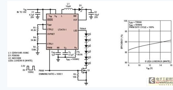
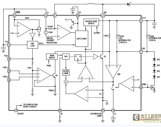
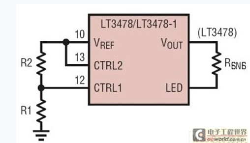
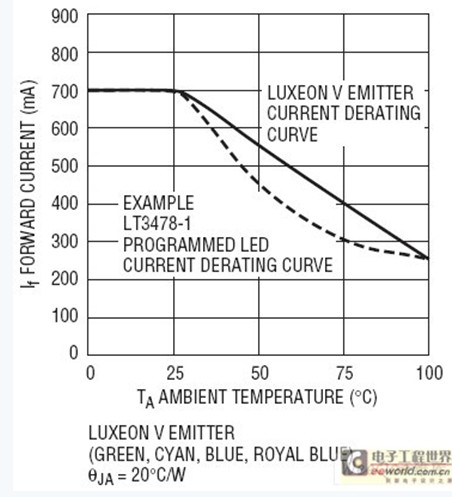
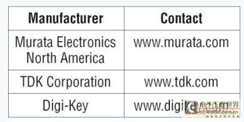
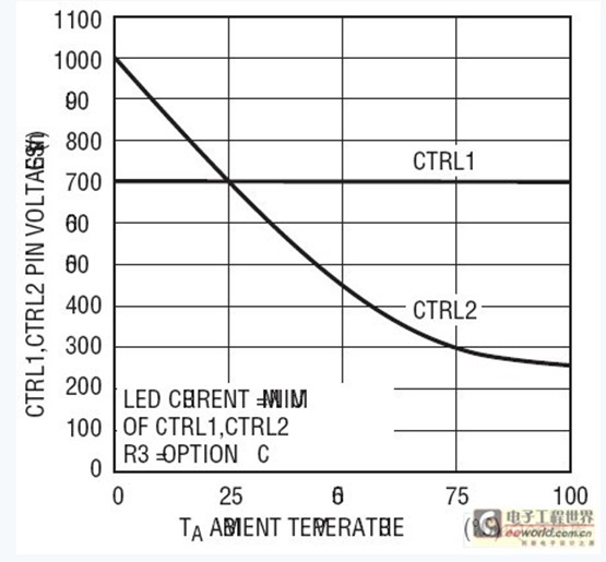
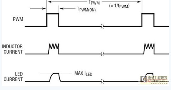
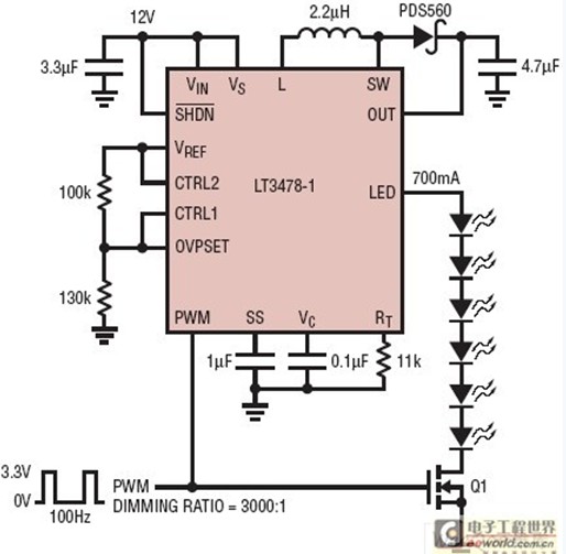
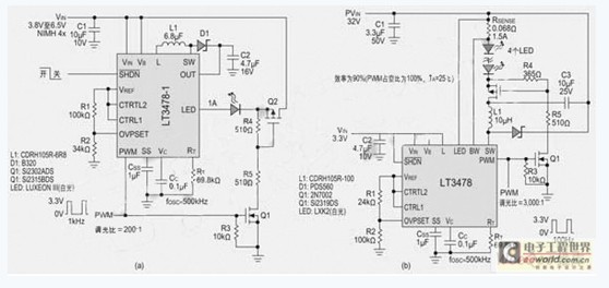
One of the reasons for the popularity of LED lighting solutions is that LEDs can achieve a wide dimming range with simple current control, such as automotive dashboards and aircraft cockpits where the ambient illumination may be very low. Wide PWM dimming range. Linear Technology's LT3478 and LT3478-1 are single-chip step-up DC/DC converters that use a constant current to drive high-brightness LEDs over a wide range of settings. In addition to the optional 10:1 analog dimming range, the LT3478 and LT3478-1 feature a 3000:1 PWM dimming range to maintain LED color. The LT3478 and LT3478-1 are easy to use and have programmable features designed to optimize performance, reliability, form factor and total cost. These devices operate in boost, buck, and step-down LED driver topologies. The amount of LED current they can provide depends on the topology, up to 4A. Ideal for high-power LED applications, including automotive and avionics, the LT3478 and LT3478-1 are available in a 16-pin thermally enhanced TSSOP package with E- or Class I temperature ratings. Figure 1: Step-up LED driver circuit for automotive TFT LED backlight applications. The LT3478 and LT3478-1 operate similarly to conventional current-boost converters, but they use LED current (rather than output voltage) as the primary feedback source for the control loop. Figure 2 shows the main functions of each part. Both devices feature high-side LED current sensing for operation in both buck and boost modes. The LT3478-1 saves space and cost by integrating current sense resistors and limits the maximum LED current to 1.05A. The LT3478 uses an external sense resistor that allows a maximum programmable LED current of 4A. Figure 2: Functional block diagram of the LT3478 and LT3478-1. Set the maximum LED current Dimming current control is an important feature, but it is also important to avoid LED overdrive (beyond its maximum current rating). The LT3478 and LT3478-1 make it easy to set the maximum current and reduce the maximum current based on temperature. Figure 3: Circuit connection diagram used to set the maximum LED current. The LT3478 and LT3478-1 use the CTRL1 pin voltage to control the maximum LED current unless the device is set to reduce the maximum LED current based on temperature (using the CTRL2 pin). A simple resistor divider from VREF (see Figure 3) or an external voltage supply can be used to set the CTRL1 pin voltage, or CTRL1 can be tied directly to the VREF pin to provide maximum current. Figure 4 shows the LED current vs. CTRL1 pin voltage. Figure 4: LED current vs. CTRL1 pin voltage. Reduce maximum LED current based on temperature To ensure optimum reliability, LED manufacturers specify a maximum allowable LED current versus temperature curve (Figure 5). If the maximum LED current is not adjusted according to the temperature, it may cause permanent damage to the LED. Figure 5: LED current drop curve versus ambient temperature. Figure 6: Setting the LED current derating curve versus temperature. The LT3478 and LT3478-1 use the CTRL2 pin to reduce current. As shown in Figure 6, simply connect the CTRL2 pin to VREF through a temperature-dependent resistor divider. When the temperature rises, the CTRL2 pin voltage drops. When the CTRL2 pin voltage drops below the CTRL1 pin voltage, the maximum LED current is set by the CTRL2 pin voltage (Figure 7). The temperature at which the LED current begins to drop and the speed at which the current drops are selected by the resistor network/resistance used. Table 1 lists the website information of NTC resistor manufacturers Murata Electronics, TDK and Digi-Key. Murata Electronics Inc. specifically provided an in-circuit simulation program for selecting the desired combination of resistors (shown in Figure 6), including a catalogue describing NTC resistor specifications. Figure 5 shows an example of the LT3478-1 programming LED current drop versus temperature curve, using the alternative C shown in Figure 6, where: R4 = 19.3k, RY = 3.01k, RNTC = 22k (NCP15XW223J0SRC ). For a more detailed description of how these values ​​can be determined by hand calculations, please refer to the data sheets for the LT3478 and LT3478-1. Table 1: NTC Resistor Manufacturer/Distributor. Figure 7: CTRL1 and CTRL2 pin voltage vs. temperature. Analog dimming Many LED applications require accurate brightness control. LED brightness can be reduced simply by reducing the LED current. This method is called "analog dimming", but reducing the operating current of the LED changes the color of the LED. The LT3478 and LT3478-1 can achieve 10:1 dimming by reducing the CTRL1 pin voltage from 1V to 0.1V. PWM dimming is a better alternative if color retention is important. Figure 8: PWM dimming is done through the PWM pin. Figure 9: PWM dimming waveform, when the PWM pin is active high or low, the LED current is the maximum or 0 respectively. PWM dimming PWM dimming (Figures 8 and 9) produces a very high dimming ratio and does not cause current-dependent LED color variations. The PWM dimming of the LT3478 and LT3478-1 is achieved through the PWM pin. When the PWM pin is active high (TPWM(ON)) or low, the LED current is either maximum or zero, respectively. The on-time (or average current) of the LED is controlled by the duty cycle of the PWM pin. Since the LED is always operating under the same current conditions (the maximum current is set by the CTRL1 pin), and only the average current changes, dimming does not cause the color change of the LED. PWM dimming is not a new technology, but achieving a high PWM dimming ratio (requiring a very low PWM duty cycle) can be challenging. The LT3478 and LT3478-1 use a patented architecture to achieve a PWM dimming ratio (100Hz) of over 3000:1. The application circuit of Figure 10 can achieve a PWM dimming ratio of more than 3,000:1, provided that the PWM on-time is reduced to three switching cycles (TPWM(ON) <3.3μs when fPWM = 100Hz). 11 and 12 are corresponding relationship curves and waveforms of Fig. 10. Figure 10: Step-up LED driver circuit optimized for high PWM dimming ratio. The PWM pin is used to achieve the maximum PWM dimming ratio (PDR) that satisfies the following relationship: PWM dimming ratio = 1 / minimum PWM duty = 1 / (TPWM (ON) MIN · fPWM) The simplified waveform in Figure 10 and the criteria given below illustrate the relationship between PWM duty cycle, PWM frequency, PWM dimming ratio, and LED current: 1. For a 100Hz PWM frequency (fPWM), a PDR of 3,000 means a 3.3μs PWM turn-on time. 2. For a fixed PWM on-time, the lower the PWM frequency, the higher the PWM dimming ratio. However, there is a limit to what level of PWM frequency can be controlled, because the human eye will feel the frequency below 80Hz. 3. Increasing the programming switching frequency (fOSC) can increase the PDR, but it will result in a decrease in efficiency and an increase in internal heat generation. In general, TPWM(ON)MIN=3×1/fOSC (approximately 3 switching cycles). 4. The leakage current of the output capacitor should be minimized. When the PWM pin is low, the LT3478 and LT3478-1 turn off all circuits that draw operating current from VOUT. 5. For a wider dimming range, PWM dimming and analog dimming can be combined. TDR=PDR·ADR, where TDR=total dimming ratio, PDR=PWM dimming ratio, ADR=analog Dimming ratio. A 3000:1 PDR and a 10:1 (CTRL pin voltage of 0.1V) ADR will produce a TDR of 30,000:1. Figure 11: Curve of LED current versus PWM dimming ratio in the circuit of Figure 10. Open circuit LED protection The output voltage has a configurable maximum value to avoid damage to the LED due to disconnection (open LED) and subsequent reconnection. During the LED disconnection, the converter is variable to the open circuit and drives the output voltage to a very high level, causing damage to the internal power switch. Most LED drivers have a fixed maximum output voltage to protect the switch, but this voltage may be too high for reconnected LED strings. The LT3478 and LT3478-1 provide a programmable overvoltage protection (OVP) level to limit the output voltage based on the number of LEDs in series. The OVPSET voltage is responsible for limiting the maximum output voltage, maximum output voltage = OVPSET voltage x41. Figure 12: PWM dimming waveform of the circuit of Figure 10. The OVPSET voltage is obtained from VREF using its own resistor divider or by adding a resistor to the voltage divider used to determine the CTRL1 voltage. The OVPSET programming level should not exceed 1V to ensure that the switching voltage does not exceed 42V. High reliability: fault detection and soft start For reliable performance during hot-swap, startup, or normal operation, the LT3478 and LT3478-1 can monitor system parameters for any of the following faults: VIN<2.8V, SHDN<1.4V, inductor inrush current greater than 6A and/or The output voltage is higher than the programmed OVP voltage. Once any of the above faults are detected, the LT3478 and LT3478-1 immediately stop switching and discharge the soft-start pin (Figure 13). When all faults are removed and the SS voltage is discharged below 0.25V, the internal 12μA supply will charge the SS pin at the rate set by the external capacitor CSS. A gentle rise in the SS voltage is equivalent to a ramp up of the switch current limit until the SS voltage exceeds the VC voltage. High efficiency: independent inductor and IC power supply, can be set to fOSC, 60mΩ switch The LT3478 and LT3478-1 feature separate IC and inductor power supplies to optimize efficiency and switching duty cycle range. The inductor inrush current is sensed using the VS and L pins, independent of the VIN supply (Figure 2), which allows the VIN to be powered from the system's lowest available supply (at least 2.8V) to minimize the power switch driver. Loss of efficiency. In this way, the inductor can be powered by a power supply (2.8V to 36V) that is more suitable for the duty cycle and power requirements of the LED load. The switching frequency of the power switch can be adjusted to achieve the optimum inductor size and efficiency performance required by the system. The 60mΩ on-resistance further increases efficiency by minimizing switching losses (for high duty cycle operation). Figure 13: LT3478/LT3478-1 Fault Detection and SS Pin Voltage Timing Diagram. Summary of this article The LT3478 and LT3478-1 are ideal for boost, buck or step-down LED driver applications that require high LED current and high PWM dimming ratio. The 4.5A high peak switch current limit and the new PWM dimming architecture enable the LT3478 and LT3478-1 to provide high PWM dimming ratios up to 4A. (The Linear Technology Corporation) Figure 14: Drop-down LED driver circuit for portable photo flash applications. Edit: Nizi High Power H Series Lead Acid Battery High Rate Discharge Battery,High Energy Battery,High Output Battery,H Series Lead Acid Battery Wolong Electric Group Zhejiang Dengta Power Source Co.,Ltd , https://www.wldtbattery.com