Wewow gimbal has full series Smartphone Gimbal from one axis gimbal to two axis gimbal, Three Axis Gimbal.
Wewow gimbal can fit with 95% smartphone in the market, such Samsung, iphone, Huawei, Xiaomi, HTC, etc.
Smartphone Gimbal Smartphone Gimbal,Handheld Smartphone Gimbal,Gimbal Stabilizer For Smartphone,Professional Smartphone Gimbal GUANGZHOU WEWOW ELECTRONIC CO., LTD. , https://www.stabilizers.pl
At present, there has been a power controller that can be reduced, which allows designers to select the number of phases for a particular DC-DC converter. The scalable architecture allows several controllers to work in parallel and simultaneously. The on-chip PLL-based clock generator enables multiple devices to work synchronously.
Multi-phase topology Although the single-phase buck regulator does not have strict power limits, when the load current rises above 20A to 30A, the multi-phase converter will have obvious advantages. These advantages include: lower input ripple current, greatly reducing the number of input capacitors; the output ripple frequency is also reduced due to the equivalent multiplication of the output ripple frequency; and the temperature of the component due to the distribution of losses in more components It has also been reduced; and the height of external components has also been reduced.
Multi-phase converters are essentially multi-channel buck regulators working in parallel, their switching actions remain synchronized, the phase deviates from 360 / n degrees, where n is equal to the number of phases. The parallel connection of the converters makes the output regulation a little more complicated. This problem is easily solved with a current-mode control IC. This controller regulates the current in each inductor in addition to the output voltage.
Input ripple current When choosing the input capacitor, the key issue facing designers is the handling of input ripple current. The use of a multi-phase topology greatly reduces the input ripple current—the input capacitance of each phase only needs to handle lower amplitude input current pulses. In addition, the phase deviation also increases the equivalent duty cycle of the current waveform, resulting in a lower RMS ripple current. The ripple current values ​​listed in Table 1 illustrate the reduction in ripple current and the savings in input capacitance.
High-k dielectric ceramic capacitors provide the highest ripple current handling capability and the smallest PCB footprint. 1812-shaped ceramic capacitors each have a rated ripple current of up to 2A to 3A. For cost-sensitive designs, electrolytic capacitors are a good choice.
Reducing the output ripple voltage core power supply usually requires <2% accuracy. For a 1.2V power supply, this is equivalent to an output voltage window of ± 25mV. A technique called active voltage positioning can take advantage of this output voltage window. At light load, the converter adjusts the output voltage above the midpoint of the window, and at heavy load, adjusts the output voltage below the midpoint of the window. For the ± 25mV window, adjust the output to the high end (low end) of the window under light load (heavy load), then the entire output voltage window can be used to respond to the step load of the rise (fall).
The large load current step requires the capacitor to have a very low ESR to reduce the transient voltage. It also requires the capacitor to have a large enough capacity so that the energy stored in the main inductance is absorbed when the load jumps downward. Organic polymer capacitors have lower ESR than tantalum capacitors. Polymer capacitors have the lowest ESR and highest capacity. Ceramic capacitors have excellent high frequency characteristics, but the capacity of each device is only one-half to one-quarter of that of tantalum or polymer capacitors. Therefore, in general, ceramic capacitors are not the best choice for output capacitors.
Low-side MOSFET A 12V to 1.2V converter requires the low-side MOSFET to be turned on 90% of the time; in this case, the conduction loss is much higher than the switching loss. For this reason, two or three MOSFETs are often used in parallel. Working in parallel with multiple MOSFETs effectively reduces RDS (ON), thus reducing conduction losses. When the MOSFET is turned off, the inductor current continues to flow through the body diode of the MOSFET. Under this condition, the drain voltage of the MOSFET is basically zero, which greatly reduces the switching loss. Table 1 shows the loss of several multi-phase configurations. Note that the total loss of the low-side MOSFET decreases as the number of phases increases, thus reducing the temperature rise of the MOSFET.
When the duty cycle of the high-side MOSFET is 10%, the switching loss of the high-side MOSFET is much larger than the conduction loss. Because the high-side MOSFET only conducts in a very short time, the conduction loss is not significant. In this way, reducing switching losses is more important than reducing on-resistance. During the switching process (tON and tOFF), the MOSFET needs to withstand a certain voltage and transmission current, the product of this voltage and current determines the peak power loss of the MOSFET; therefore the shorter the switching time, the smaller the power loss. When choosing a high-side MOSFET, you should choose a device with lower gate charge and gate-drain capacitance, which are more important than low on-resistance. As can be seen from Table 1, the total loss of the MOSFET decreases as the number of phases increases.
Inductor selection The inductance value determines the peak-to-peak value of the ripple current. Ripple current is usually expressed as a percentage of the maximum DC output current. For most applications, the ripple current can be selected to be 20% to 40% of the maximum DC output.
When the core voltage is low, the decay rate of the inductor current is not as fast as the rise rate. When the load decreases, the output capacitor will be charged with excessive charge, causing overvoltage. If an inductor with a smaller value is selected (produces a larger ripple current—approximately 40%), the energy stored in the inductor transferred to the output capacitor is less and the resulting surge voltage is lower.
Heat dissipation design Table 1 gives an estimate of the heat dissipation requirements when using different phase numbers. In a forced convection cooling system that provides 100LFM to 200LFM, the single-phase design requires a relatively large heat sink to obtain a thermal resistance of 0.6 ° C / W. In the four-phase design, the thermal resistance can be increased to 2 ° C / W. This thermal resistance can be easily achieved without a heat sink and airflow from 100LFM to 200LFM.
Table 1. Comparison of synchronous buck regulators designed with different phase numbers and their important parameters. In this example, 12V to 1.2V, 100A buck regulators Number of Phases 1 2 4 8 Current per phase 100A 50A 25A 12.5A Input capacitor, 3A rated Ripple current 31.6A 22A 15.8A 11.2A Number required 11 8 6 4 H / S MOSFET RMS ripple current 31.6A 15.8A 7.9A 3.9A Package size DPAK DPAK SO-8 SO-8 Number required 2 2 (1 / ph) 8 (2 / ph) 8 (1 / ph) Power dissipaTIon (each) 22W 1.8W 0.32W 0.22W Total power dissipaTIon 4.4W 3.6W 2.5W 1.76W L / S MOSFET RMS ripple current (each) 94.8A 47.4A 23.7A 11.9A Package Size DPAK DPAK SO-8 SO-8 Number required 3 2 (1 / ph) 8 (2 / ph) 8 (1 / ph) Power dissipaTIon (each) 6W 12W 1.4W 1W Total power dissipaTIon 18W 24W 11.2W 8W COUT 470µF, 10m Number required 7 7 7 7 VSS ripple 22mV 11mV 5mV 1mV Heatsink capacity 0.6 ° C / W 1 ° C / W 2 ° C / W 4 ° C / W Estimated efficiency 69 77 85 89
Design example Figure 1 is a four-phase DC-DC converter configured with the MAX5038. The remote voltage detector (VSP to VSN pin) of the MAX5038 master controller detects the output voltage and simultaneously provides a signal (DIFF) to the EAN input of the master / slave controller to achieve parallel operation. The MAX5038 master controller also provides a clock output (CLKOUT) for another MAX5038 slave controller. Leave the PHASE pin floating to make the internal clock of the slave controller and the CLKIN signal produce a 90 ° phase shift. By setting the proper gain, the error amplifier can also realize the active voltage positioning function. Using precision resistors to set the gain can ensure accurate load balancing. The output of the error amplifier (EAOUT) determines the load current of each phase. Each current loop is compensated at the CLP1 and CLP2 pins (not shown). After proper compensation, it can provide a very stable output under most input and load conditions. 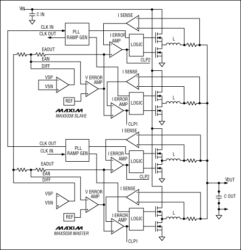
Figure 1. Four-phase design example using two MAX5038s. The master controller performs voltage telemetry and clock generation functions, and the slave controller expands the output current and works synchronously with the master controller. Conclusion Multi-phase synchronous DC-DC converters can effectively drive ASICs or processors operating from 1V to 1.5V and consuming 100A or higher. They solve many basic problems, including capacitor ripple current, MOSFET power consumption, transient response, and output voltage ripple.
Abstract: Today's high-performance ASICs and microprocessors may consume up to 150W of power. For supply voltages from 1V to 1.5V, the current required by these devices can easily exceed 100A. Using a multi-phase DC-DC converter to provide power to these devices is a more feasible solution.