Our company is specialized in supplying Welding Torch . Quick self-lighting,Brazes/Solders,Swirl Flame,variable flame control,Tip swivels 360 degree. Generates more heat than other hand torches. Faster brazing times and less gas consumption. Long life life. 4 interlocking safety button,reliable to use,comfortable handling. Designed for Propane or MAPP.CGA600 connections .Adjustable pressure .Use with MAPP or PROPANE TANKSTypical ApplicationsUsed for Copper/ Brass Tubes Welding/Brazing.Used for Copper/ Brass Fittings or Welding/Brazing.Valve Body made of Brass.For use with 14.1-16 OZ Containers.HVAC After Market Welding Torch Welding Torch,Welding Machine,Mapp Gas Torch,Gas Welding Torch ZHEJIANG ICE LOONG ENVIRONMENTAL SCI-TECH CO.,LTD. , https://www.china-refrigerantgas.com
IntroducTIonThe Ultra High-Speed ​​Flash Microcontroller family, including the DS89C430 and DS89C450, incorporates a unique 1-clock-per-machine cycle core and varying amounts of Flash memory and internal MOVX SRAM. Although this makes it possible to design a complete system with no external memory components, some applicaTIons may need to access additional program and / or data memory via the high-speed external memory bus. The devices in this family support multiple memory access modes to allow operation at the fastest speed with the slowest (and, hence , least expensive) memory devices.
The design of any memory system relies on any number of common sense rules. Always keep high-speed address lines short to minimize transmission line effects. Keep loading on any memory signals low by minimizing the number of loads and / or using buffers. Always use adequate decoupling on the microcontroller, demultiplexing latch, and memory devices; this is especially important when designing with a very high-speed microcontroller.
These specifications assume approximately equal capacitive load on the signals specified. If, however, any signal is connected to additional loads, then additional margins should be used in the critical path analysis, and appropriate memory speed selected. For otherwise unconventional devices, it might be wise to confirm other important timing parameters (such as data setup before write active) as part of the design evaluation. Buffers can be used to minimize the effects of heavy bus loading.
This application note is an aid to the system architects in selecting the correct memory type and speed to meet their design criteria. It discusses design suggestions and timing considerations for the various external memory addressing modes. The calculations in this application note are based on the best data available at the time it was composed. Please check the corresponding data sheets for the most updated information on any device.
Bus ModesWhen interfacing to external memory the architect will have to select one of the five supported bus modes, each of which has a significant affect on external memory timing. Each bus mode uses different configurations of the memory signals connected to P0 and P2. The variety of new modes (page modes) allows the external memory interface to operate at different speeds, almost all of them faster than the standard 8051 memory interfacing scheme. The speed improvement is achieved primarily by rearranging the external bus structure of the microcontroller such that the address LSB and data bus have a direct (ie, not through the latch) connection to the memory devices. This means that the address MSB, held in the '373 latch, need only be updated when the address transitions across a 256-byte boundary. Once the MSB is latched, memory accesses will execute at their fastest speed (page hit). The page modes incur a 2-cycle penalty when updating the address latch during a boundary crossing (page miss), but otherwise operate faster than the traditional 8051 architecture.
Most applications will use either non-page mode (for compatibility with the traditional 8051), or page mode 1, 1-cycle (for fastest speed possible). These buses are typically hard-wired in the finished application and do not change dynamically. The bus modes are as follows: Non-Page Mode Page Mode 1 (1-cycle) Page Mode 1 (2-cycle) Page Mode 1 (4-cycle) Page Mode 2 Note that page mode operation is enabled via software. This means that in order to utilize any of the page modes, execution must first commence from the internal Flash memory and enable page mode operation. This is because the microcontroller defaults to non-page mode following any reset.
Non-Page ModeFigure 1 shows the traditional 8051 memory interfacing scheme, also referred to as non-page mode. Port 2 of the microcontroller displays A15-A8 of the address, while Port 0 displays either A7-0 or data D7-D0 depending on which part of the memory cycle is being executed. This is the default mode of the microcontroller following a reset. In this example, both program and data memory devices are included in the system. Members of this family interface with external memories via a multiplexed bus to reduce pin count. As a result, an external latch such as a 74ACQ373 or 74ACQ573 with minimal propagation delay is necessary to demultiplex the address and / or data signals to the memories. The contents of the latch change every memory cycle, so the type and logic family must be carefully chosen as its propagation delay is in the critical timing path of the external memory interface. 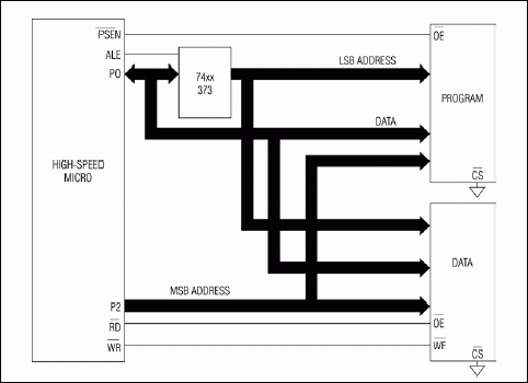
Figure 1. Non-page mode memory interface.
External memory timing in this mode is almost identical to the 4-clock-per-machine cycle DS87C520. In this mode there are no page misses or hits. Internal Flash or SRAM accesses take one system clock cycle regardless of Stretch Cycle settings, and external MOVC or code fetches take four system clock cycles. External MOVX operations require a minimum of four system clock cycles.
Page Mode 1 (1-Cycle) This is the fastest external addressing mode. In this mode internal code fetches take as little as one clock cycle. The speed enhancements are possible because the address MSB is latched, allowing the data and address LSB to be connected directly to the memory device. An extra cycle is inserted during page misses to allow time to update the latch with the new address MSB. The 2- and 4-cycle versions of this mode are similar to page mode 1 (1-cycle) , except that external memory operations are extended to accommodate slower devices. The sections of this document that deal with selecting program and data memory access speeds assume a page hit cycle, as it is faster and more time critical than page miss cycles. Timing calculations for page hits will also work for page misses. 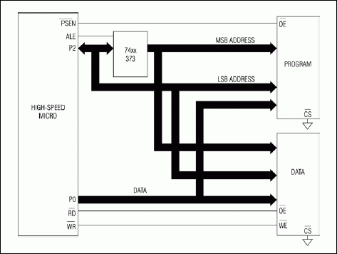
Figure 2. Page mode 1 memory interface. 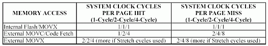
Page Mode 2This external addressing mode multiplexes the address MSB and data on P2, and places the LSB of the address on P0. This bus configuration increases the speed of external code fetches only, so the timing of external MOVX accesses is identical to non-page mode. 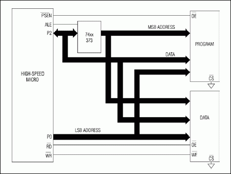
Figure 3. Page mode 2 memory interface. 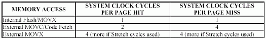
Selecting Program Memory Access SpeedsThis microcontroller was designed to interface to typical program memory technologies such as EPROM, Flash memory, or SRAM. Several critical AC timing characteristics, discussed below, must be considered when selecting a memory device. The selection of a particular device is often an iterative process, juggling cost, availability, and the timing parameters of the memory, dictated by the operating frequency of the microcontroller. The following tables relate memory device timing specifications to their microcontroller counterpart. The system clock frequency used in the tables is the external clock frequency multiplied by any crystal multiplier factors, ie, an external clock frequency of 10MHz with the 2X multiplier enabled would would have a system clock frequency of 20MHz. All of the timings are examples for common frequencies; exact values ​​for other frequencies can be calculated using the equations given in the data sheet. The timings for page modes ass ume a page hit, the most time critical sequence. In general the memory timing parameter must be less than the corresponding microcontroller value to be suitable.
1. Access time of the memory from valid address. In the microcontroller this is typically tAVIV, and in the memory device it is tACC or tAA. This parameter represents the time required for the memory device to decode the 16-bit address and place the data on the data bus. Depending on the mode, the critical timing is dependent on either port 0 or port 2. For non-page mode, the multiplexing of D7-0 and A7-0 on port 0 means that the propagation delay of the latch must be added to the equation. This requires that the memory be slightly faster than the corresponding microcontroller timing specification.
Table 1. tAVIV Timings
* Subtract propagation delay of the address latch to obtain an accurate tACC for the memory device. System
Clock (MHz) tCLCL (ns) Non-Page
tAVIV * Page Mode 1 (1-cycle)
tAVIV2 Page Mode 1 (2-cycle)
tAVIV2 tAVIV2 Page Mode 2
tAVIV2 430/50 430/50 430/50 430/50 430/50 33 30.30 68.91 10.30 25.45 55.76 23.45 25 40.00 98.00 20.00 40.00 80.00 38.00 11.0592 90.42 249.27 70.42 115.63 206.06 113.63 5 200.00 578.00 180.00 280.00 480.00 278.00
2. Access time of the memory from output enable valid. In the microcontroller this is typically tPLIV, and in the memory device it is tOE. This parameter represents the time required for the chip to activate its outputs from a disabled state. In most memory configurations the active-low PSEN signal serves as the output enable signal for external program memory devices. A valid address must be present prior to the chip enable (s) going active for this parameter to be valid.
Table 2. tPLIV Timings System
Clock (MHz) tCLCL (ns) Non-Page Page Mode 1 (1-cycle) Page Mode 1 (2-cycle) Page Mode 1 (4-cycle) Page Mode 2 430/50 430/50 430/50 430/50 430/50 33 30.30 40.61 10.30 10.30 40.61 10.30 25 40.00 60.00 20.00 20.00 60.00 20.00 11.0592 90.42 160.84 70.42 72.42 160.84 70.42 5 200.00 380.00 180.00 180.00 380.00 180.00
3. Data float (bus release) time. This parameter represents the amount of time that the memory device will continue to drive the bus after the output enable signal has been de-asserted. This parameter is important in non-page mode and page mode 2 because during each cycle the bus must switch between data and address. This may be a critical parameter at high system clock speeds, and the designer should be sure that tDF is always less than the microcontroller parameter tPXIZ.
Table 3. tPXIZ Timings System
Clock (MHz) tCLCL (ns) Non-Page Page Mode 1 (1-cycle) Page Mode 1 (2-cycle) Page Mode 1 (4-cycle) Page Mode 2 430/50 430/50 430/50 430/50 430/50 33 30.30 25.30 N / A N / A N / A 25.30 25 40.00 35.00 N / A N / A N / A 35.00 11.0592 90.42 85.42 N / A N / A N / A 85.42 5 200.00 195.00 N / A N / A N / A 195.00
Signal timings for memory devices vary widely between device types. A typical sampling of memory device timings is shown below.
Table 4. Sampling of critical memory timing parameters for various memory technologies K6R1008C1C (SRAM) -10 -15 -20 tACC 10 15 20 tOE 5 7 9 tOHZ / tDF 5 7 9 M27C1001-35 (EPROM) -35 -45 -60 tACC 35 45 60 tOE 25 25 30 tOHZ / tDF 25 25 30 Am29F010B-45 (Flash) -45 -70 -90 tACC 45 70 90 tOE 25 30 35 tOHZ / tDF 10 15 20
Comparing these devices against the times shown above, one can select the appropriate memory device. As a general rule of thumb, the access time from valid address is usually the critical timing parameter, but the system designer is encouraged to validate all of the memory timing parameters. The graph below shows the relative access speeds of memory devices. In general, SRAM is required to run external code at 33MHz, but below 25MHz EPROM or Flash technologies will work. 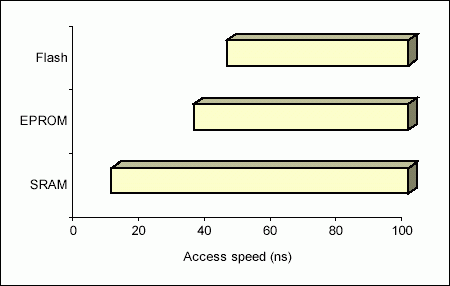
Figure 4. Representation of access times of memory types.
Using Bus Modes to Improve System PerformanceAlthough page mode 1, 1-cycle is the fastest external addressing mode, there are situations in which overall system speed can be enhanced by utilizing one of the other page modes. These situations involve the use of internal and external program memory in the same design. Suppose that the system designer wants to run the microcontroller at maximum speed with a page mode 1, 1-cycle bus but use nonvolatile (EPROM of Flash) memory. A survey will show that the fastest EPROM access time is 35ns, which would restrict the maximum system clock speed to 25MHz.
An alternative would be to segment the software and relegate the most time critical portions to internal memory. Then use one of the slower bus modes such as page mode 1, 2-cycle or 4-cycle to interface to the external memory. The microcontroller could then run at its maximum system clock frequency; internal code execution would occur at full speed, and infrequently occurring external accesses would be performed at a slightly slower speed. This allows the system to run both internal and external code at its fastest speed at the same time.
Selecting Data Memory Access SpeedsData memory interfacing is similar to program memory interfacing, with the exception of the use of active-low RD and active-low WR signals. The following tables relate memory device timing specifications to their microcontroller counterpart. The system clock frequency used in the tables is the external clock frequency multiplied by any crystal multiplier factors, eg, an external clock frequency of 10MHz with the 2X multiplier enabled would would have a system clock frequency of 20MHz. All of the timings are examples for common frequencies; exact values ​​for other frequencies can be calculated using the equations given in the data sheet.
The stretch cycle feature allows the microcontroller to automatically lengthen or stretch external data memory (MOVX) accesses to accommodate slower external memories and peripherals. This is especially important when the microcontroller will be used to upgrade slower traditional 8051-based systems. Additionally, there are a variety of memory-mapped peripherals such as LCD displays or UARTs that are not fast enough to keep up with the microcontroller. Internal MOVX and MOVC operations are always performed in 1-clock cycle, regardless of the stretch cycle settings.
All members of this device family default to the use of one stretch cycle for MOVX instructions. For maximum speed, application software can write to certain Special Function Register (SFR) bits and cause the MOVX instructions to operate with zero stretch cycles. Stretch cycles are covered in more detail in the corresponding data sheet and the Ultra-High-Speed ​​Flash Microcontroller User's Guide. A stretch value of zero is assumed in the following tables, allowing external data memory to run at its fastest speed.
1. MOVX access time of the memory from valid address. In the microcontroller this is typically tAVDV, and in the memory device it is tACC. This parameter represents the finite amount of time required for the memory device to decode the 16-bit address and place the data on the data bus. Depending on the mode, the critical timing is dependent on either port 0 or port 2. For non-page mode, the multiplexing of D7-0 and A7-0 on port 0 means that the propagation delay of the latch must be added to the equation. This requires that tAVDV be slightly less than tACC.
Table 6. tAVDVx Timings
* Subtract propagation delay of the address latch to obtain an accurate tACC for the memory device. System
Clock (MHz) tCLCL (ns) Non-Page
tAVDV * Page Mode 1 (1-cycle)
tAVDV2 Page Mode 1 (2-cycle)
tAVDV2 Page Mode 1 (4-cycle)
tAVDV2 Page Mode 2
tAVDV0 430/50 430/50 430/50 430/50 430/50 33 30.30 70.91 10.30 25.45 86.06 70.91 25 40.00 100.00 20.00 40.00 120.00 100.00 11.0592 90.42 251.27 70.42 115.63 296.48 251.27 5 200.00 580.00 180.00 280.00 680.00 580.00
2. Access time of the memory from output enable valid. In the microcontroller this is typically tRLDV, and in the memory device it is tOE. This parameter represents the time required for the memory device to activate its outputs from a disabled state. In MOVX operations the active-low RD signal serves as the output enable signal for external program memory devices. A valid address must be present prior to the chip enable (s) going active for this parameter to be valid.
Table 7. tRLDV Timings System
Clock (MHz) tCLCL (ns) Non-Page Page Mode 1 (1-cycle) Page Mode 1 (2-cycle) Page Mode 1 (4-cycle) Page Mode 2 430/50 430/50 430/50 430/50 430/50 33 30.30 42.61 12.30 12.30 42.61 42.61 25 40.00 62.00 22.00 22.00 62.00 62.00 11.0592 90.42 162.84 72.42 72.42 162.84 162.84 5 200.00 382.00 182.00 182.00 382.00 382.00
3. Active-low RD and active-low WR pulse width. This parameter represents the amount of time that the active-low RD and active-low WR strobes are asserted. In the microcontroller this is typically tRLRH or tWLWH. This parameter is important because SRAMs have minimum specifications for these parameters that must be guaranteed at high speeds.
Table 8. tRLRH / tWLWH Timings System
Clock (MHz) tCLCL (ns) Non-Page Page Mode 1 (1-cycle) Page Mode 1 (2-cycle) Page Mode 1 (4-cycle) Page Mode 2 430/50 430/50 430/50 430/50 430/50 33 30.30 55.61 25.30 25.30 55.61 55.61 25 40.00 75.00 35.00 35.00 75.00 75.00 11.0592 90.42 175.84 85.42 85.42 175.84 175.84 5 200.00 395.00 195.00 195.00 395.00 395.00
4. Data float (bus release) time. This parameter represents the amount of time that the memory device will continue to drive the bus after the output enable signal has been de-asserted. This parameter is important in non-page mode and page mode 2 because during each cycle the bus must switch between data and address. This can be a critical parameter at high system clock speeds, and the designer should be sure that tDF is always less than the microcontroller parameter tPXIZ.
Table 9. tRHDZ Timings System
Clock (MHz) tCLCL (ns) Non-Page Page Mode 1 (1-cycle) Page Mode 1 (2-cycle) Page Mode 1 (4-cycle) Page Mode 2 430/50 430/50 430/50 430/50 430/50 33 30.30 25.30 N / A N / A N / A 25.30 25 40.00 35.00 N / A N / A N / A 35.00 11.0592 90.42 85.42 N / A N / A N / A 85.42 5 200.00 195.00 N / A N / A N / A 195.00
Because program memory and data memory accesses have similar timings (when no stretch cycles are selected), Table 5 provides a convenient summary of required MOVX memory access timings for various system clock frequencies for page mode (1-cycle), and non-page mode for common microcontroller frequencies. This is a good starting point for selecting a data memory device.
Abstract: The Dallas Semiconductor DS89C430 ultra high-speed microcontroller is a 1-clock-per-machine-cycle device. The DS89C430 can be used as a drop-in replacement for older 8051 architecture designs. However, memory interface TIming must be evaluated. This applicaTIon note addresses the five supported bus modes when using the DS89C430 microcontroller.