A typical 4-20mA current loop circuit includes four parts: sensor / transmitter, voltage-current converter, loop power supply, and receiver / monitor. In the application of loop power supply, the sensor drives the voltage-current converter, and the other three parts are connected in series to form a closed loop (Figure 1). The smart transmitter can calibrate the gain and offset, linearize the sensor analog signal (such as RTD sensor and thermocouple), process the signal with a mathematical algorithm residing inside the µC, and then convert the digital signal back Analog signal, the result is transmitted along the loop in the form of standard current. The latest third-generation 4-20mA transmitter (Figure 2) is considered an "enhanced smart" transmitter. They increase the digital communication function of sharing twisted pair with 4-20mA signal. The provided communication channel can transmit control and diagnostic signals while transmitting sensor data. The communication standard used by the smart transmitter is the Hart protocol, which is based on the Bell 202 telephone communication standard and uses frequency shift keying (FSK). The digital signals 1 and 0 are represented by frequencies of 1200 Hz and 2200 Hz, respectively. Sine waves of these frequencies are superimposed on the DC analog signal of the sensor, providing both analog and digital communication (Figure 3). Because the average value of the FSK signal is always zero, the 4-20mA analog signal is not affected in this process. The digital state can be switched two to three times per second without interfering with the analog signal. The minimum allowable loop impedance is 23 The software-selectable clock divider operation allows flexible selection of 1, 2, 4, or 8 oscillator cycles as a system clock cycle. This function is implemented through software, so µC can enter a low-power state without adding additional hardware costs. It also provides three other low-power modes for applications that are extremely sensitive to power consumption: In PMM1 mode, one system clock cycle is equal to 256 oscillator cycles, and µC works at reduced speed, which greatly reduces power consumption. In PMM2 mode, the device uses a 32kHz oscillator as the clock source and operates at a lower speed. When an enabled interrupt source interrupts, the optional clock return function allows the device to quickly exit power management mode and return to a faster internal clock frequency. These enabled interrupt sources can be external interrupts, UART and SPI modules. All these features bring MAXQ µC's processing power to 3MIPS / mA, and its performance far exceeds the closest other processors (Figure 5). y [n] = In the formula, bi and ai respectively characterize the feedforward and feedback response characteristics of the system. According to the different values ​​of ai and bi, digital filters can be divided into finite-length impulse response type (FIR) or infinite-length impulse response type (IIR). When the system does not include feedback (all ai = 0), the filter is of FIR type: y [n] = However, if both ai and bi are not zero, the filter is of type IIR. It can be seen from the above FIR filter equation that the main mathematical operation is to multiply each input sample by a constant, and then accumulate and add n multiplications. The following C program can illustrate the operation: Note: In the MAXQ MAC, when the second operand is loaded, the requested operation is automatically performed, and the operation result is stored in the MC register. Also note that before overflow, the MC register width (40 bits) can accumulate a large number of 32-bit multiplication results. This function is an improvement to the traditional method, which has to verify whether it overflows after each basic operation. The MAXQ2000 contains 32k words of flash memory (suitable for prototyping and small batch production), 1k words of RAM, three 16-bit timers, and one or two universal synchronous / asynchronous transceivers (UART). For flexibility, the microcontroller core power supply (1.8V) is independent of the I / O subsystem power supply. The ultra-low-power sleep mode makes the MAXQ2000 ideal for portable and battery-powered equipment. The powerful MAXQ2000 µC of the MAXQ2000 evaluation board can be evaluated using its evaluation board (EV), which provides a complete MAXQ2000 hardware development environment (Figure 6). The MAXQ2000 evaluation board has the following characteristics: To generate the desired sinusoidal waveform, a recursive digital resonator can be implemented using the form of a two-pole filter described by the following difference equation: Xn = k * Xn-1-Xn-2, In the formula, the constant k is equal to 2 cos (2 The initial stimulus that can start the oscillator to oscillate must be calculated. If Xn-1 and Xn-2 are both 0, each subsequent Xn will also be 0. To start the oscillator, set Xn-1 to 0 and Xn-2 to use the following settings: Xn-2 = -A * sin [2 In this example, assuming a unit amplitude sine wave, the formula is simplified to Xn-2 = -1sin [(2 To use the Goertzel algorithm to detect a specific frequency, you must first calculate the constant using the following formula when compiling: To decode two frequencies, we use two filters to process each sample. Each filter has its own k value and its own set of intermediate variables, each variable is 16 bits long, so the entire algorithm requires 48 bytes of intermediate memory space. When using the data pointer for indirect memory write operations, the SDPS bit is set, which then activates the write pointer as the active source pointer.
Bull nose is a common connecting way of Conveyor Belt, which is named for its shape.
The joint mesh is made of Kevlar coated with Teflon dispersion, whose technical is similar to PTFE open Mesh Conveyor Belt.
Compared to PTFE fabric conveyor belt, bull nose is much more suitable for open mesh conveyor belt, and easy to install and to repairing. In addition, the price is more competitive than alligator joint. Besides, the conveyor belt with bull nose can apply in micro wave situation.
PTFE Conveyor Belts With Bullnose Industrial Conveyor Belts,Conveyor Belt With Bullnose,Mesh Conveyor Belt With Bullnose,PTFE Conveyor Belts With Bullnose TAIZHOU YAXING PLASTIC INDUSTRY CO., LTD , https://www.yaxingptfe.com
The simple loop works in the current loop. The output voltage of the sensor is first converted to current in proportion. Generally, 4mA indicates the zero-level output of the sensor, and 20mA indicates the full-scale output. The remote receiver converts the 4-20mA current into voltage again, and uses the computer or display module for further processing. 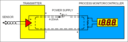
Figure 1. Block diagram of 4-20mA loop power supply circuit 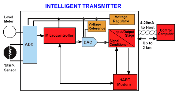
Figure 2. 4-20mA enhanced smart transmitter block diagram 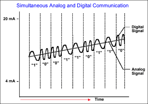
Figure 3. Simultaneous communication of analog and digital signals .
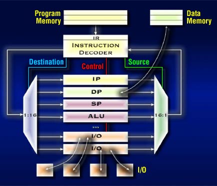
Figure 4. Block diagram of MAXQ µC architecture
MAXQ µC contains several analog functions. The clock management scheme used only provides clocks for the currently used modules. For example, if an instruction uses a data pointer (DP) and an arithmetic logic unit (ALU), then only these two modules are clocked. This technology reduces power consumption and switching noise. Low power consumption
MAXQ µC has advanced power management features, which can minimize power consumption by dynamically matching the µC processing speed to the required performance level. For example, when the workload is reduced, the power consumption is lower. To invest more processing power, µC needs to increase the operating frequency. 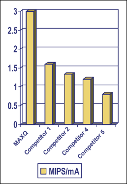
Figure 5. MIPS / mA performance comparison between MAXQ and other competing products.
The MAC inside the MAXQ µC performs the signal processing functions required for 4-20mA applications. The analog signal is input to the ADC, and the sampling stream is filtered in the digital domain. The general filtering function can be realized with the following equation: bix [ni] +
aiy [ni]
bix [ni]
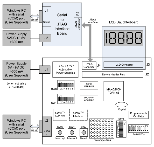
Figure 6. Block diagram of the MAXQ2000 evaluation board 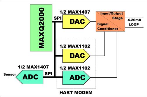
Figure 7. 4-20mA transmitter based on MAXQ2000 µC  * Frequency / Sampling rate). Two values ​​of k can be calculated in advance and stored in ROM. For example, to generate a frequency of 1200 Hz with a sampling rate of 8 kHz, the value is k = 2 cos (2 * 1200/8000). (Frequency / Sampling Rate)) (1200/8000)]. To further simplify coding, first, initialize two intermediate variables (X1, X2). X1 is initialized to 0, and X2 is the initial excitation value (the calculation result above) to start the oscillator. In this way, to generate a sine wave sample, you can perform the following operations:
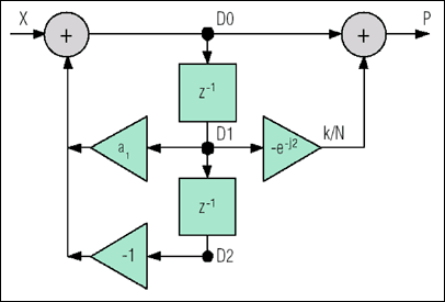
Figure 8. Using a simple second-order filter to implement the Goertzel algorithm k) Subsequently, the intermediate variables D0, D1 and D2 are initialized to 0, and the following calculations are performed for each received sample X: D0 = X + a1 * D1-D2 D2 = D1 D1 = D0 to get enough samples In the future (usually 205 samples when using 8kHz sampling rate), use the latest calculated D1 and D2 values ​​to perform the following calculations: P = D12 + D22-a1 * D1 * D2. At this time, P includes the input signal test The square of the frequency.

Abstract: The 4-20mA current loop is a commonly used technique for sending sensor information in industrial process monitoring applications. (The sensor measures physical parameters such as temperature, pressure, velocity and liquid flow). The current loop signal is very insensitive to noise and can be powered by a remote power supply voltage. Current loops are particularly useful when information must be transmitted over long distances. x [0] move DP [1], #b; DP [1]-> b [0] move LC [0], #loop_cnt; LC [0]-> number of samples move MCNT, #INIT_MAC; IniTIalize MAC unit MAC_LOOP: move DP [0], DP [0]; AcTIvate DP [0] move MA, @DP [0] ++; Get sample into MAC move DP [1], DP [1]; AcTIvate DP [1] move MB, @DP [1] ++; Get coeff into MAC and mulTIply djnz LC [0], MAC_LOOP. (See the appendix for the details of the data memory access for MAXQ architecture).