Traditional tools for debugging PCBs include: time domain oscilloscopes, TDR (time domain reflectometry) oscilloscopes, logic analyzers, and frequency domain spectrum analyzers, but none of these tools can provide an overall reflection of the PCB board. data. This article describes how to obtain complete PCB electromagnetic information using the EMSCAN EMI scanning system and how to use this information to aid in design and debugging.
EMSCAN has a spectrum scanning function and a spatial scanning function. The results of the spectral scan allow us to have a general idea of ​​the spectrum produced by the EUT: how many frequency components there are, and what is the magnitude of each frequency component. The result of the spatial scan is for a frequency point, which is a topographic map with color representing the amplitude. We can see the dynamic electromagnetic field distribution of a certain frequency point generated by the PCB in real time.
Full band scanning
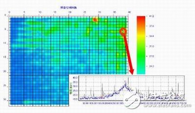
When performing the spectrum/spatial scanning function, the working PCB is placed on the scanner, and the PCB is divided into 7.6 mm & TImes by the raster of the scanner; a small grid of 7.6 mm (each small cell contains an H field probe), and the execution is performed. After full-band scanning of each probe (frequency range can be from 10 kHz to 3 GHz), Emscan finally gives two graphs, which are synthetic spectrograms.

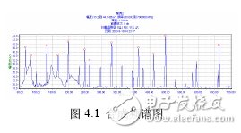
(Fig. 1) and synthetic space map (Fig. 2)
The spectral/spatial scan yields the full spectrum data for each probe in the entire scan area. After performing a spectrum/spatial scan, you can get the electromagnetic radiation information of all frequencies in all spatial locations. You can imagine the spectrum/spatial scan data of Figure 1 and Figure 2 as a bunch of spatial scan data (each spatial scan is different) The frequency, which you can control for different displays), can also be thought of as a bunch of spectral scan data (each spectrum scans from a different physical location on the PCB, which can be one or several grids). You can:
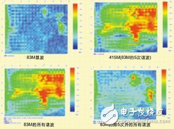
1. View the spatial distribution of the specified frequency point (one or more frequencies) as you would a spatial scan result, as shown in Figure 3.
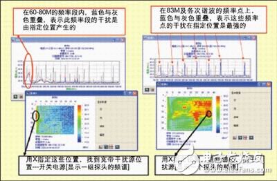
2. View the spectrogram of the specified physical location point (one or more rasters) as you would a spectrum scan, as shown in Figure 4.
Each spatial distribution map of Fig. 3 is a spatial abdominal view of the frequency point by a specified frequency point. It is obtained by specifying the frequency point with &TImes; in the uppermost spectrogram in the figure. You can specify a frequency point to view the spatial distribution of each frequency point, or you can specify multiple frequency points, for example, specify all harmonic points of 83M to view the total spectrum.
In the spectrogram of Fig. 4, the gray portion is the total spectrum map, and the blue portion is the spectrum map at the specified position. The location of the interference source is found by specifying the physical location on the PCB with &TImes; comparing the spectrogram (blue) and the total spectrogram (gray) produced at that location. As can be seen from Figure 4, this method can quickly find the location of the interference source for both wideband interference and narrowband interference.
Quickly locate electromagnetic interference sources
The “interference source†can also be located using a spectrum analyzer and a single near-field probe. Here, a "fire-fighting" method is used to make a metaphor. The far-field test (EMC standard test) can be compared to "detecting a fire". If the frequency point exceeds the limit value, it is considered to be "a fire has been discovered." The traditional "spectrum analyzer + single probe" solution is generally used by EMI engineers to detect "Which part of the chassis is coming out of the chassis." After detecting the flame, the general EMI suppression method is to use shielding and filtering to put " The flames are inside the product. EMSCAN allows us to detect the source of the source of interference - "fire", but also to see the "fire", the source of interference.
When using EMSCAN to check the EMI problem of the whole machine, the tracking process from "fire" to "fire" is generally used. For example, scan the chassis or cable first, check which part of the interference comes from, further trace the inside of the product, which PCB is causing interference, and further trace the device or wiring.
It can be clearly seen from Fig. 4 that using "complete electromagnetic information", it is very convenient to locate the electromagnetic interference source, which can not only solve the problem of narrow-band electromagnetic interference, but also be effective for the problem of wide-band electromagnetic interference.
The general method is as follows:
(1) Look at the spatial distribution of the fundamental wave and find the physical position with the largest amplitude on the spatial distribution map of the fundamental wave. For wideband interference, specify a frequency in the middle of the broadband interference (for example, a wideband interference of 60MHz-80MHz, we can specify 70MHz), check the spatial distribution of the frequency point, and find the physical location with the largest amplitude.
(2) Specify the location and see the spectrogram at that location. Check that the amplitude of each harmonic point at this location coincides with the total spectrum. If they coincide, the specified location is the strongest place to generate these disturbances. For wideband interference, check if the location is the maximum location for the entire wideband interference.
(3) In many cases, not all harmonics are generated in one position, and sometimes even and odd harmonics are generated at different positions, and it is also possible that each harmonic component is generated at a different position. In this case, you can find the location with the strongest radiation by looking at the spatial distribution of the frequency points you care about.
(4) The means of taking the strongest radiation is undoubtedly the most effective in solving EMI/EMC problems.
This EMI troubleshooting method that truly tracks the "source" and propagation path allows engineers to eliminate EMI problems at the lowest cost and speed. In a measured case of a communication device, radiation interference is radiated from the telephone line cable, and it is obviously not feasible to add shielding or filtering means to the cable, so the engineer is at a loss. After the above-mentioned tracking scan with EMSCAN, the processor board was finally replaced by a few dollars, and several filter capacitors were installed to solve the EMI problem that the engineer could not solve.
Quick positioning circuit fault location
As the complexity of the PCB increases, the difficulty and workload of debugging increases. With an oscilloscope or logic analyzer, only one or a limited number of signal lines can be observed at the same time. There may be thousands of signal lines on the PCB. Engineers can only find problems by experience or luck. The problem.
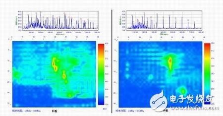
If we have the "complete electromagnetic information" of the normal board and the fault board, by comparing the data of the two, we find the abnormal spectrum, and then use the "interference source positioning technology" to find out the location of the abnormal spectrum. Find the location and cause of the fault.
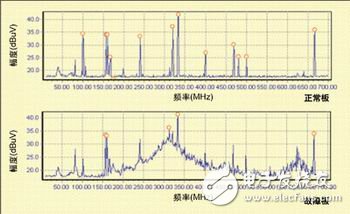
Figure 5 shows the spectrum of the normal board and the fault board. By comparison, it is easy to find that there is an abnormal broadband interference on the fault board.
Then find the location of the "abnormal spectrum" on the spatial distribution map of the fault board, as shown in Figure 6, so that the fault location is located at a grid (7.6mm & TImes; 7.6mm), the problem can be very Quickly diagnosed.
Application case for evaluating PCB design quality
A good PCB needs to be carefully designed by engineers. The issues to consider include:
(1) Reasonable cascading design
In particular, the arrangement of the ground plane and the power plane, as well as the design of the layer where the sensitive signal line (clock signal) and the signal line (address line and data line) generating a large amount of radiation are located. There are also ground planes, power plane divisions, and routing of signal lines across the divided areas.
(2) Maintain as continuous signal line impedance as possible
As few vias as possible; as few as possible right-angle traces; and as small a current reflow area as possible, can produce less harmonics and lower radiation intensity.
(3) Good power supply filtering
Reasonable filter capacitor type, capacitance, quantity, and placement, as well as a reasonable stacking of ground plane and power plane, can ensure that electromagnetic interference is controlled in the smallest possible area.
(4) As much as possible to ensure the integrity of the ground plane
As few vias as possible; reasonable via safe spacing; reasonable device layout; reasonable via arrangement to maximize ground plane integrity. Conversely, dense vias and excessive via safety margins, or unreasonable device layout, can severely affect the integrity of the ground plane and power plane, resulting in a large amount of inductive crosstalk, common mode radiation, and circuitry. More sensitive to outside interference.
(5) Finding faults in signal integrity and electromagnetic compatibility
Under the premise of ensuring the normal function of the device (guaranteeing signal integrity), the rising edge and falling edge time of the signal are increased as much as possible, and the amplitude and harmonic quantity of the electromagnetic radiation generated by the signal are reduced. For example, it is necessary to select a suitable damping resistor, a suitable filtering means, and the like.
Previously, we did not have a simple and scientific means to evaluate the design quality of PCBs and the design level of PCB designers. Using the complete electromagnetic field information generated by the PCB, the PCB design quality can be scientifically evaluated. Using the complete electromagnetic information of the PCB, the design quality of the PCB can be evaluated from the following four aspects: 1. Number of frequency points: the number of harmonics. 2. Transient interference: Unstable electromagnetic interference. 3. Radiation intensity: The magnitude of the electromagnetic interference at each frequency point. 4. Distribution area: The size of the distribution area of ​​electromagnetic interference on the PCB at each frequency point.
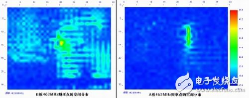
In the example below, the A board is an improvement of the B board. The schematic of the two boards and the layout of the main components are identical. The results of the spectrum/space scan of the two plates are shown in Figure 7:
From the spectrum diagram of Figure 7, it can be seen that the quality of the A board is significantly better than that of the B board because:
1. The number of frequency points of the A board is significantly less than that of the B board;
2. The amplitude of most of the frequency points of the A board is smaller than that of the B board;
3. The transient interference of the A board (no frequency points marked) is less than that of the B board.
It can be seen from the space diagram that the total electromagnetic interference distribution area of ​​the A board is much smaller than that of the B board. Let's look at the electromagnetic interference distribution at a certain frequency point. From the distribution of electromagnetic interference at a frequency point of 462 MHz shown in Fig. 8, the amplitude of the A-plate is small and the area is small. The B plate has a large amplitude and a particularly wide distribution area.
A large number of test cases prove that this method of using the complete electromagnetic field information generated by the PCB to evaluate the quality of PCB design is completely reasonable. We can see the design level of the designer from the quality of PCB design, and also provide designers with the most intuitive guidance to continuously improve the design level.
Summary of this article
The complete electromagnetic information of the PCB allows us to have a very intuitive understanding of the PCB as a whole, which not only helps engineers solve EMI/EMC problems, but also helps engineers debug PCBs and continuously improve the quality of PCB design. Similarly, there are many applications for EMSCAN, such as helping engineers solve electromagnetic sensitivity problems and so on.
Wifi Antenna
-
The Description of wifi Antenna
-
When selecting the antenna, it is necessary to pay attention to whether the connector of the antenna matches the connector of the connected device. Generally, SMA and TNC are used for WIFI
To use on the router, but on the 2.4 G wireless monitoring equipment fittings, if match, also can achieve the enhancement effect of the wireless signal transmission Magnetic antenna base, can suck on metal surfaces, makes the antenna signal is stronger Plug and play, without any additional conditions, but the antenna gain and directional property management are key points to consider.
-
The first standard WIFI antenna products were made by LTCC process, because of its width and general performance. Abroad, Airgain has launched a standard antenna with high temperature resistance and plastic seal, which is used in laptop computers, and a series of WiFi antennas with magnetic dielectric in mobile phones have been launched in China.
-
The Picture of wifi Antenna
-

Wifi Antenna ,Wifi Antenna for PC ,Wifi Antenna for Router ,Wfi Antenna outdoor ,Wifi Antenna Indoor
Yetnorson Antenna Co., Ltd. , https://www.yetnorson.com