The network communication industry in 2012 seems to be unsurpassed, but in fact it is surging, then a lot of things have happened in the network communication industry in 2012, and it is basically driven by technology, what new technologies are there in 2012, and in 2013 What new technological trends will there be, through the complex and complicated, and listen to me one by one. Year-end review of 2012 network technology inventory The booming mobile Internet has spawned 802.11ac preterm birth According to 740 million WLAN chip shipments in 2011 and 1.1 billion smart business terminal devices this year, we see that smartphones and tablets now have WiFi as a standard feature, but 2G and 3G have become optional features. It seems that WiFi has been accepted by the public. What trends will WLANs have in 2013? Relevant data shows that in 2013, the number of people going out of office will reach 1.2 billion, while mobile office workers will account for 35%. They have also developed rapidly in the enterprise network. More and more employees use their own smart terminal equipment to work, and efficiency Greatly improved, which triggered BYOD trend. This year is the fastest year for the development of the 802.11ac wireless protocol. Although the agreement has not yet been finalized, there are several manufacturers that have released products for the Gigabit wireless routers supporting 802.11ac in the home. The integration of enterprise networks into wired and wireless integration is accelerating. Network manufacturers are actively working on how to meet the service quality requirements of high-bandwidth business such as high-definition video streaming and multimedia, so that enterprise users can enjoy high-quality wireless services. Huawei first released a wireless AP that supports 802.11ac in July this year. Network manufacturers have paid close attention to the progress of 802.11ac for a while. On November 29th, Ruijie Networks released its X-sense "smart". Antenna's 802.11ac Gigabit wireless AP product-RG-AP530. On December 6, Huawei announced the industry's first enterprise-grade 802.11ac AP product in Beijing. The product includes two AP and AC products. Aruba also released It supports 802.11ac wireless controller (AC) products. Although network manufacturers have actively released their wireless routers and wireless APs that support 802.11ac, the resistance to their development is that most terminals do not support 802.11ac. Currently, the only products that support 802.11ac are ASUS notebooks. The wireless network card that supports 802.11ac, only the newly released UnionPay, but the time to market has not yet been determined. I believe that with the determination of the 802.11ac wireless protocol and the continuous efforts of chip manufacturers, a variety of new products supporting 802.11ac have been developed, so as to make it more active. BYOD meets at every meeting and talks about hot topics for the whole year This year ’s industry ’s hottest topic is none other than BYOD. For BYOD brings new opportunities and challenges, each manufacturer provides its own solution, but as BYOD diversity changes, companies and network vendors have their views on this. It is also different. BYOO represents a phenomenon that is personalized, mobile, and intelligent. People's lives and work are connected by a variety of intelligent terminals. The office is not limited to the traditional pC machine in the office. The own device has become a A trend that blurs the boundaries between office and life, giving the office a better experience. BYOO is not a one-off phenomenon. It is a new office model that emerges with the development of advanced communications and IT technology. Corporate office has experienced from "fixed" scenarios to "mobile", from location restrictions to everywhere. Three development stages (this article mainly explores the development of mobile office): offline mobile office, online mobile office, and intelligent mobile office (BYOD). For this hottest and hottest technology, it has attracted the attention of many manufacturers and enterprises, but enterprises are most concerned about data security issues, device loss, device management and other issues. I believe that as companies continue to understand BYOD, they will definitely More and more companies will deploy BYOD solutions. At the same time, as BYOD technology matures, BYOD solution providers will also provide a variety of solutions to meet different customer needs. New technology, only SDN success or failure hero OpenFlow originated from the Clean Slate project team of Stanford University. They separated the two functional modules of data forwarding (data plane) and routing control (control plane) of traditional network equipment, and standardized interfaces through a centralized controller (Controller) Management and configuration of various network devices, then this will provide more possibilities for the design, management and use of network resources, thereby making it easier to promote network innovation and development. So, they proposed the concept of OpenFlow, based on the programmable features that OpenFlow brings to the network, Nick and his team further proposed the concept of SDN (Software Defined Network). To give an inappropriate example, SDN technology is equivalent to stripping away the management setting system and router of each home router. In the past, each router had its own management system, but with SDN, a management system can be used on all brands of routers. If the current network system is a functional machine, and the system and hardware are bundled together at the factory, then SDN is the Android system, which can be installed and upgraded on many smart phones, and at the same time install more and more powerful mobile apps (SDN Application layer deployment). Although OpenFlow and SDN are not specifically created for network virtualization, the standardization and flexibility they bring bring unlimited possibilities to the development of network virtualization. We believe that OpenFlow / SDN does bring many opportunities for network transformation and innovation. From a horizontal perspective, SDN is a double-edged sword for traditional network vendors. With this sword, you can occupy more markets in the market. If you do n’t use it well, it will become a hot topic on the Internet. In the same way as for the demise of network vendors, of course, for traditional network vendors, if you don't "reform" your own lives, there will naturally be others working on your behalf. Who will be the leader in the SDN era, maybe time is the best prover. Dinosaurs with well-developed limbs are about to go extinct, and creatures with developed minds rule the earth. This is evolution. 10 Gigabit exchange bumps forward development depends on the future 2010 was the most milestone year in the field of Ethernet technology. On June 17, IEEE officially approved the IEEE 802.3ba standard, which marked the official departure of the commercial road for 40G / 100G Ethernet. It took two and a half years from the formal establishment of the working group in early 2008 to the formal approval and publication of the standard. It seems that everything is in the plan, but the road to the formulation of the 40G / 100G standard is far from superficial. smoothly. Those who are familiar with the Ethernet standard will first discover the "alternative" Ethernet rate of 40G in the standard. 10M-》 100M-》 1000M (1G)-》 10 Gigabit (10G) (Figure 2), Ethernet has always defined a higher interface rate at a rate of 10 times, 40G-this is the first time for Ethernet Breaking this rule, so it is difficult! The standards of 40G / 100G related fields were fully implemented in 2010, which opened a new field of Ethernet technology development. Since 2009, the industry's leading equipment manufacturers have launched and claimed to provide support for 40G / 100G ports and applications, but as a new technology, some key technological breakthroughs and breakthroughs will be involved in each link of its research and development and deployment. Innovation, which also brings a series of new challenges and problems to chip developers, equipment manufacturers and end users. 1. Router / switch processing capabilities, including total machine capacity, port density, high-speed look-up table, flow management, thermal design and energy-saving design 2. High-speed interface of dedicated message processing chip, including high-speed SerDes, high-speed large-capacity cache, etc. 3. (Super) long-distance transmission, how to use existing optical fiber and other infrastructure to achieve single-wavelength 40G / 100G ultra-long-distance transmission, including the use of more complex modulation methods, the use of EDFA, and the FEC algorithm with higher gain, etc. Although 40G / 100G faces many difficulties, but with the continuous drive of demand, I believe that with the efforts of many manufacturers, we will be able to overcome these difficulties, solve all problems encountered, and achieve excellent results in the 10G field. The mega-era really came.
4 Layer PCB
Four-layer circuit board is a kind of Printed Circuit Board. It is made of four layers of glass fibre, which can reduce the cost of PCB.
There are also great differences between the 2-layer and 4-layer PCB. For details, please click: What's the difference between 2 layer and 4 layer PCBs?
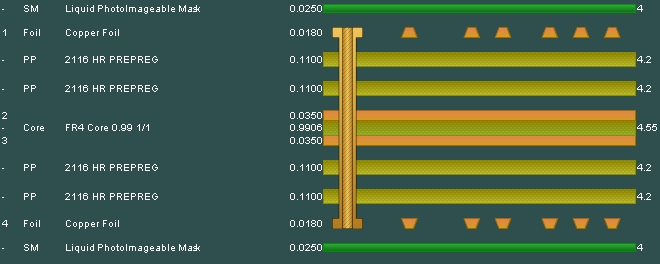
4 layer PCB stackup include two inner layers, inner layer 1 and 2, are sandwiched between the top and bottom layers. From top to bottom, the 4-layer PCB stackup like below ,The top, i.e. the signal layer (0.0014 in. width) is followed by a prepreg layer with a thickness of 0.0091 in. and dielectric constant of 4.2. The top layer is copper material. The prepreg layer is followed by inner layer 1 (0.0014 in.), referred to as the plane. A core sublayer is part of inner layer 1, which has a width of 0.037 in. This is followed by inner layer 2, which is another plane layer made with 1 oz. copper and is 0.0014 in. thick. Another prepreg sublayer constituting two sheets that are 0.0091 in. thick forms part of inner layer 2. The final layer, the bottom layer, is also 0.0014 in. thick, and is a signal layer as well. Interconnects are soldered and placed on the top and bottom layers.
The standard 4-layer PCB stack is shown below, and GND and VCC can be switched according to the layer with more signals.
If you don't want to connect all the ground pins through the hole, there will be different stacks and wide power routing on the signal plane.
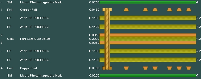
4 LAYER 0.8 MM STANDARD BUILD
4 LAYER 1.6 MM STANDARD BUILD
0.4mm, 0.6mm, 0.8mm, 1.0mm, 1.2mm, 1.6mm, 2.0mm, 2.4mm, Please contact us if your board exceeds these.
Cost of four layer PCB is higher than double sided PCB because of complexity of design and higher sensitivity. The better quality of signals, achieved by reducing distortion and propagation levels, is also a factor. Because of the higher levels of signal integrity and reduced interference levels, more manufacturers prefer four layer PCB.
4 Layer PCB Printed Circuit Board,4 Layer PCB,4 Layer PCB Board,4 Layer Printed Circuit Board JingHongYi PCB (HK) Co., Limited , https://www.pcbjhy.com
What is 4 layer PCB?
Compared with Double Sided PCB , multi-layer PCB have many advantages. They can be designed more compactly. They can greatly improve noise resistance and make layout easier.
4 layer PCB stackup and thickness

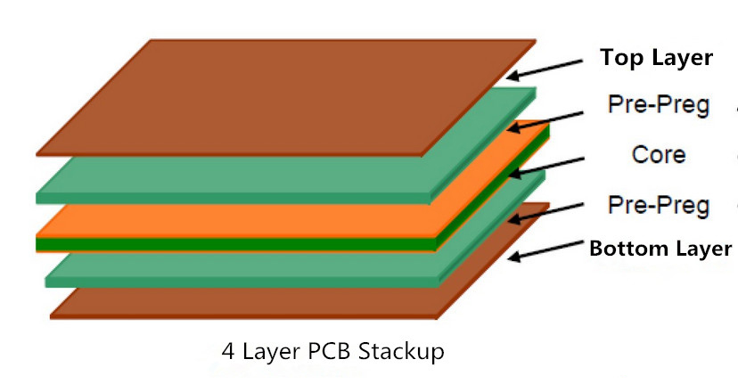
4-layer PCB has two stacking forms
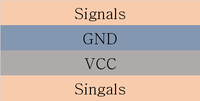
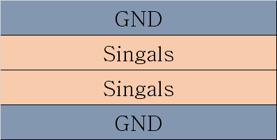
For the following reasons, this may be a better stack to use a four-layer PCB:
When the high-speed signal changes the reference plane, there should be a nearby path for its return current to move between the two reference planes. Using two horizons, you can do this by connecting two planes directly to a single channel. For grounding and power layers, the connection must be made through capacitors, which usually require two through-holes and one capacitor. This means worse signal integrity and more circuit board occupancy. On the other hand, having a power plane can reduce the voltage drop on the power rail, thereby releasing the space on the signal layer.
PCB Board Thickness
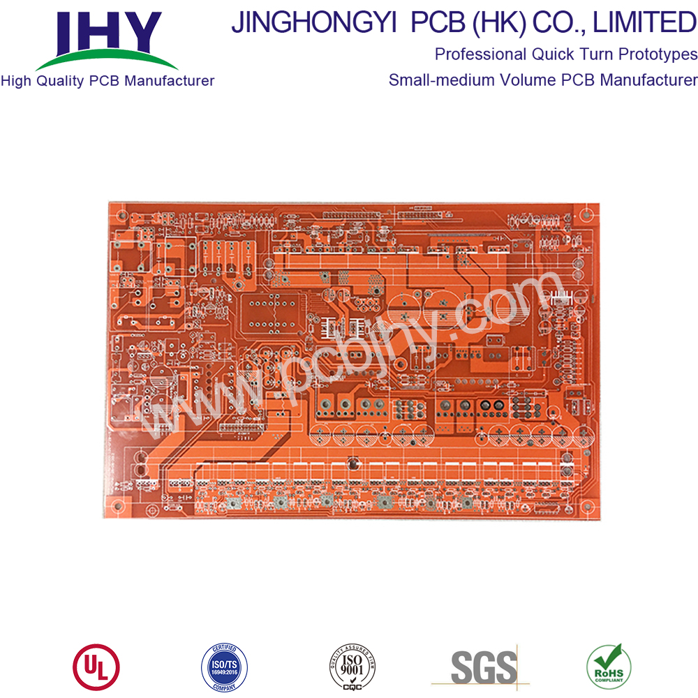
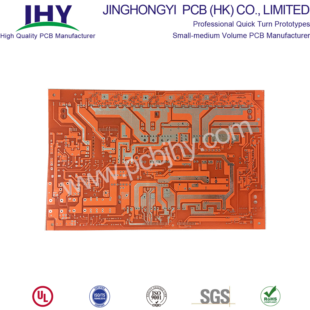
4 layer PCB Prototype
4-layer circuit board prototyping refers to the trial production of Printed Circuit Boards before mass production. It is mainly used for electronic engineers to design circuits and complete PCB Layout, then to carry out small-scale trial production process to the factory, that is, proofing PCB. The production quantity of four-ply proofing generally has no specific boundaries. Generally, engineers call it proofing before product design has not been confirmed and test has been completed.
Notices for proofing of four-layer circuit boards
The precautions for the production of four-layer PCB samples generally include two groups, one is the Engineer group, the other is the PCB Sample manufacturer.
As a group of engineers, the matters needing attention in proofing are as follows:
1. Choose proofing quantity carefully to control cost effectively.
2. Specially confirm device packaging to avoid proofing failure due to packaging errors.
3. Conduct comprehensive electrical inspection to improve the electrical performance of PCB board.
4. Make good signal integrity layout, reduce noise and improve PCB stability.
As a manufacturer of four-layer circuit boards, the precautions are as follows:
1. Check PCB files carefully to avoid data problems.
2. Conduct process approval in an all-round way and process configuration with self-manufacturer.
3. Control production quantity, reduce cost and maintain quality.
4. Communicate with customers who need samples to prevent accidents in advance.
4 layer PCB price and cost
We specialize in Quick Turn PCB services with an industry leading turnaround time as fast as 24 hours. Three low-cost options for a small number of PCB prototyping needs. At the same time, we also provided Flexible PCB , Rigid- Flex PCB , Metal Core PCB , High-TG PCB, Aluminum PCB , PCB Stencils, PCB Assembly Services and so on. Using the same high-tech equipment as our full-service PCB, it can be manufactured quickly and with virtually no limits.
4 layer PCB Manufacturing
We provide a full range of PCB functions to meet all your PCB needs. At present, we accept five PCB file formats (gerber file,.Pcb,.Pcbdoc.cam or.brd file format) for PCB manufacturing. But if you design a circuit board using Sprint-Layout software, you can send the. LAy6 file to us to manually generate the Gerber file.
JingHongyi PCB can provide you with multi-layer PCB board that meets RoHS standard. With laminated material, it can match high temperature in assembly process. It is important to remember that some lead-free assembly processes will require laminated substrates to withstand temperatures exceeding 260 degrees Celsius or 500 degrees Fahrenheit over a longer period of time. To solve this problem, we have high temperature laminates in stock, so that our customers can meet the higher temperature cycle requirements of some lead-free assembly applications.
Min. Order Quantity: 1 pcs
Material: FR-4
Finished Copper: 1oz/2oz/3oz(35μm/70μm/105μm)
Inner Layer Copper Thickness:1oz/1.5oz(35μm/50μm)
Silkscreen: White, Black, None
Surface Finishing: HASL with lead, HASL lead free, Immersion gold, Hard Gold ,OSP...
Shape: Custom Shape
100% Quality control
When making circuit boards, and after they are finished, we will test and inspect them strictly to ensure that the product reaches 100% eligibility rate. Preferential prices and higher quality have always been our constant pursuit:
Videos for 4 layer PCB design and manufacturing