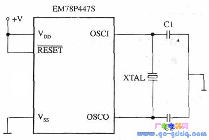
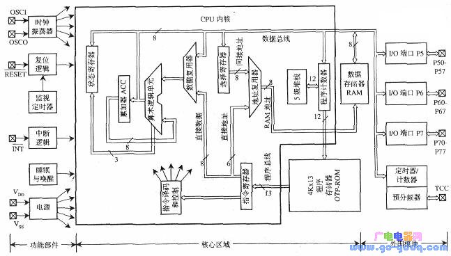
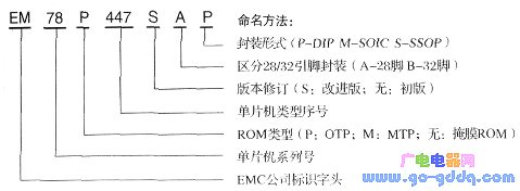
First, let's explore the performance characteristics of the EM78P447S microcontroller. The EM78 series is a family of 8-bit microcontrollers built using a low-power, high-speed CMOS process. This tutorial will focus on the EM78P447S, which features OTP (One-Time Programmable) memory. We'll cover its functional characteristics, internal structure, program and data memory, interrupt system, I/O ports, timer/counter, watchdog timer, clock oscillator, and reset system. The key performance features of the EM78P447S include: Some terms mentioned above will be further explained as we go through the details of each component. Next, let's look at the pin configuration of the EM78P447S. The pinout and logic symbols of the EM78P447S are shown in the figure above. The function of each pin is detailed in Table 1. As seen from Figure 1, the A-type version reduces four pins (P54–P57) compared to the B-type, while the rest remain compatible. This makes development easier when upgrading from A to B type. The EM78P447S has either 28 or 32 pins, each serving different functions. However, they can be categorized into four main groups: This classification helps simplify the understanding of the chip’s layout. Third, let's examine the internal structure of the EM78P447S. The internal block diagram shows the core components of the microcontroller. The CPU core is the heart of the chip, surrounded by program and data memory. Peripheral modules such as timers, interrupts, and I/O ports are also included. The design allows for flexibility in application development. Now, let's break down the key components within the core area: 1. Data bus: 8-bit wide, used for transferring data between components like RAM, ALU, and registers. 2. Program bus: 13-bit wide, for fast instruction fetching from program memory. 3. Program memory (ROM): Stores user programs and fixed data. 4. Program counter (PC): Generates address codes for instruction retrieval. 5. Instruction register: Holds the current instruction and decodes it into operations. 6. Instruction decoding and control logic: Decodes instructions and generates control signals. 7. Arithmetic Logic Unit (ALU): Performs arithmetic and logical operations. 8. Accumulator (ACC): A central register used for most data operations. 9. Status register (STATUS): Tracks operation results like carry or zero flags. 10. Data memory (RAM): Stores intermediate data during program execution. 11. Data multiplexer: Selects operands from RAM or instruction code. 12. Address multiplexer: Determines the address for data memory access. 13. Indirect addressing register (RSR): Holds addresses for indirect memory access. 14. Hardware stack: Saves program breakpoints during subroutine calls. 4. Key Features and Their Functions (1) Clock Oscillator: Generates clock pulses for internal circuits. A typical setup involves connecting a crystal between OSCI and OSCO with two capacitors. (2) Reset Logic: Ensures the MCU resets properly during power-up or manual reset. The simplest connection is to tie the RESET pin to VDD. (3) Power Supply Circuit: Distributes power between VDD and VSS. Works within 2.2V to 5.5V range. (4) Watchdog Timer (WDT): Monitors program execution. If the program crashes, WDT triggers a reset. (5) Interrupt Logic: Enables the MCU to handle unexpected events by temporarily pausing the main program and executing an interrupt service routine. (6) Sleep and Wake-up Logic: Reduces power consumption by putting the MCU into sleep mode, and wakes it up when needed. For more detailed explanations of these features, refer to dedicated sections with practical examples. 5. Peripheral Modules and Their Functions The EM78P447S includes several peripheral modules: FRP Pultruded Profiles,frp profiles,grp pultruded profiles,frp pultruded sections,pultruded profile Hebei Dingshengda Composite Material Co., Ltd. , https://www.frpdsd.com
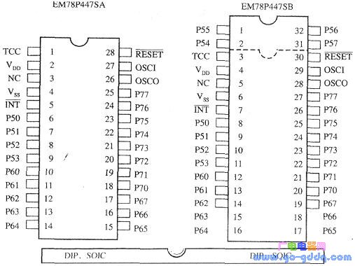
Pin name
Types of
The main function
RESET
I
Manual reset input. Schmitt trigger input. Resets MCU when low. Connect to VDD when unused.
TCC
I
Timer/Counter input. Schmitt trigger. Leave unconnected when not in use.
INT
I/O
External interrupt input. Triggered on falling edge.
OSCI
I
Crystal oscillator input. Provides clock signal for MCU.
OSCO
I/O
Oscillator output. Usually connected to a crystal between OSCI and OSCO.
VDD
-
Positive power supply.
Vss
-
Ground or negative power supply.
P50–P53
I/O
Lower 4-bit I/O port. Used in EM78447A.
P54–P57
I/O
Upper 4-bit I/O port. Full 8-bit I/O in EM78447B.
P60–P67
I/O
8-bit I/O port.
P70–P77
I/O
8-bit I/O port.
NC
Not connected.
Note: Some pins have additional functions that will be discussed in detail later.