High-power electronic power devices are repotted into an integrated module according to a certain combination of functions. Semiconductor Module Devices,Power Semiconductor Device,Semiconductor Cooling Devices,Diode Module YANGZHOU POSITIONING TECH CO., LTD. , https://www.yzpst.com
A power semiconductor module is a combination of certain functions and modes, and a power semiconductor module is a high-power electronic power device that is re-potted into a whole according to a certain function combination. Power semiconductor modules can achieve different functions according to the different components in the package. Power semiconductor modules can be used as air-cooled modules with air-cooled heat dissipation, and water-cooled modules with water-cooled heat dissipation.
It is characterized by simple installation, convenient use and maintenance, small size and light weight.
Typical applications in AC/DC motor control, various rectifier power supplies, industrial heating control, dimming, non-contact switches, electric welding machines, motor soft start, reactive power compensation, frequency converters, UPS power supplies, battery charging and discharging, etc.
In harsh environments, external interfaces must be galvanically isolated to improve safety, functionality, or immunity. This is especially true for the analog front end in data acquisition modules used in industrial measurement and control systems, as well as for digital interfaces between processing nodes.
Low Voltage Differential Signaling (LVDS) is a high-speed interface commonly used in high-performance converters and high-bandwidth FPGAs or ASICs. Its differential signaling makes it highly resistant to electromagnetic interference (EMI), as the mutual coupling between the inverting and non-inverting signals helps cancel out external noise. Adding isolation to LVDS interfaces provides a transparent solution that can be seamlessly integrated into existing signal chains for high-speed and precision measurement and control applications.
**What options are available today?**
For galvanic isolation of converters and processor interfaces, standard digital isolators offer a faster, more robust, and reliable alternative to optocouplers. However, typical LVDS data rates—often reaching hundreds of Mbps—are higher than what most standard digital isolators can support, which usually max out at around 150 Mbps.
To meet the demand for higher bandwidth isolation, system designers have turned to custom solutions involving deserialization or separation schemes using transformers and capacitors. These approaches increase both cost and design complexity, with deserialization sometimes requiring additional FPGAs for isolation.
Transformers and capacitors require careful signal conditioning of LVDS signals, and the resulting application-specific solutions often necessitate AC-balanced coding. Fiber optic communication links are another option, but they are typically more suitable for several Gbps due to their high cost and complexity.
Figure 1 illustrates the various options for high-speed isolation, showing the value proposition relative to the maximum speed of each solution.
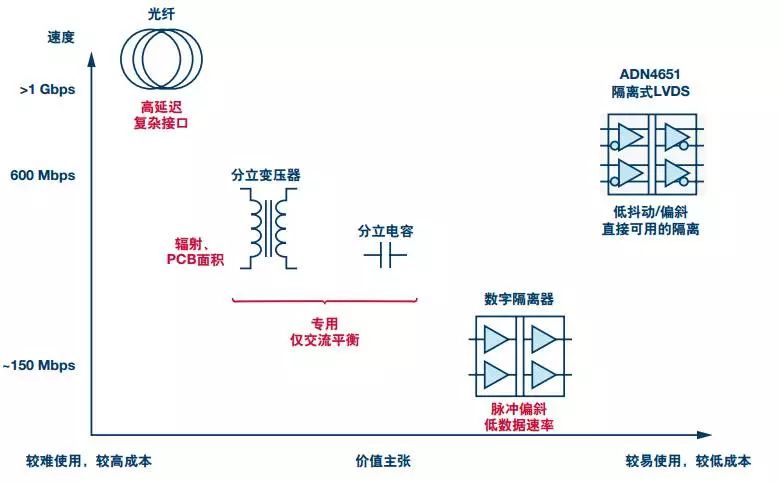
**Figure 1: The relationship between the value proposition of the isolator implementation and the isolator speed**
As a comparison, Analog Devices has introduced directly available LVDS isolators such as the ADN4650, ADN4651, and ADN4652, which use iCoupler® technology to support speeds up to 600 Mbps.
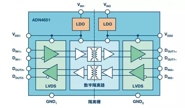
**Figure 2: ADN4651 600 Mbps LVDS Isolator Block Diagram**
These devices feature TIA/EIA-644-ALVDS-compatible I/O and a fully differential signal chain, offering high noise immunity and low radiation. They provide two isolated LVDS channels, one for receive (ADN4651) or transmit/receive (ADN4650). The internal high-speed circuit operates at 2.5 V, and an on-chip low-dropout regulator (LDO) supports a single wide-body SOIC package even with a 3.3 V supply.
**Are these new LVDS isolators a directly available solution?**
To ensure compatibility with converter interfaces or interprocessor links running at up to 600 Mbps, the ADN465x family includes ultra-low jitter precision timing. At 600 Mbps, the unit interval (UI) is only 1.6 ns, so minimizing edge jitter is critical to allow the receiving device enough time to sample the bits. The ADN465x has a total jitter of 70 ps or less, which is under 5% of the UI at 600 Mbps, assuming a bit error rate of 1 x 10^-12.
**How to quantify jitter?**
The simplest way to measure jitter is to use a differential probe to capture the LVDS signal pair, triggering on both rising and falling edges and setting the oscilloscope to infinite persistence. This overlays the transitions, allowing you to measure the crossover point. The width of this crossover corresponds to peak-to-peak jitter or time interval error (TIE).
Some jitter comes from random sources like thermal noise, known as random jitter (RJ). The peak-to-peak jitter observed on the oscilloscope depends on the run time, and as the run time increases, the histogram tail rises. Deterministic jitter (DJ), on the other hand, is bounded and includes pulse skew, data-dependent jitter (DDJ), and inter-symbol interference (ISI).
Pulse skew results from differences in propagation delay between high-to-low and low-to-high transitions, visible as offset crossovers. DDJ comes from varying propagation delays at different frequencies, while ISI is caused by previous transitions affecting the current one.
To estimate total jitter (TJ@BER) at a specific bit error rate, RJ and DJ are calculated based on the TIE distribution. A common model is the Double Dirac model, which assumes a Gaussian distribution convolved with two Dirac delta functions. While some deterministic jitter may affect the Gaussian component, combining RJ and DJ still provides a reliable estimate of TJ@BER.
The ADN4651 specifies RJ, DJ, and TJ@BER separately, ensuring these values remain within limits across power, temperature, and process variations.
**How do different LVDS interfaces rely on precise data transitions?**
A typical receiver can tolerate 10% to 20% UI jitter. For example, isolating an LVDS port with the ADN465x allows an industrial backplane to safely extend over cables between PLCs and I/O modules. At lower data rates (e.g., 200 Mbps) and with high-speed connectors and shielded twisted pairs, cable lengths of several meters are possible.
ADC interfaces often use LVDS for source-synchronous data transmission, where the clock is sent alongside data on other LVDS channels. The ADN4650’s low channel-to-device and inter-device skew (≤300 ps and ≤500 ps, respectively) is beneficial for maintaining synchronization. Data transfer occurs on both rising and falling clock edges to achieve double data rate (DDR), and the low pulse skew of ≤100 ps supports clock synchronization.
Isolating the ADC sample clock ensures that the analog front end can be isolated using an external clock source. Any jitter on the clock adds to aperture jitter, reducing measurement quality. The ADN465x has a typical additive phase jitter of only 376 fs, preserving measurement accuracy even with added isolation.
At 600 Mbps, error-free transmission, 300 MHz clock synchronization, and maximum ADC performance are demonstrated in the reference design CN-0388 using the AD7960 (18-bit, 5 MSPS SAR ADC).
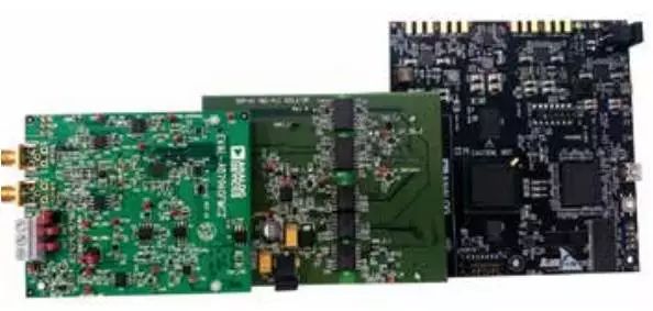
**Figure 4: ADN4651 isolation circuit for the AD7960 and SDP-H1**
The existing ADC evaluation platform between the ADC board and the high-speed SDP-H1 platform is isolated using a riser card that transparently isolates the analog front end. The software remains unchanged, and evaluations confirm that performance matches that of a non-isolated platform.
**What other applications can benefit from LVDS isolation?**
Beyond isolated analog front ends and industrial backplanes, LVDS isolation offers opportunities in various applications. For instance, video signals sent to flat panel displays often use LVDS, while HDMI uses similar differential signaling. Although isolation is not typically required, it can protect users or equipment in medical imaging or external display ports in industrial PCs.