1 Introduction
GPS attracts many users around the world with its high precision, all-weather, global coverage, convenience and flexibility, and high quality and low price. The wide application of GPS has changed the way people work, improves work efficiency, and brings huge economic benefits. Here, a design scheme of a handheld GPS positioning system based on the EM411 GPS receiving module and the PIC18F2550 microcontroller is proposed. The system uses a dot matrix character LCD to display and receive GPS satellite data, and uses the SD card to record the received GPS information, thereby realizing the GPS data to be imported into the electronic map.
2 Introduction to the NEMA Agreement
Currently, GPS uses the NMEA-0183 protocol as the standard for transmitting and receiving data. NMEA-0183 is a standard developed by the National Ocean Electronics Association (NaTIonalMarine Electronics AssociaTIon) for the unified marine navigation specification, which has become an international one. The format is based on the compatibility of NMEA-180 and NMEA-0182. Various device interfaces and communication protocol definitions such as GPS, depth sounder, and compass orientation system have been added, and some specific vendors are allowed to communicate custom protocols for their devices. All data in the NMEA-0183 format data string is represented by ASCII text characters. The data transfer begins with "$" followed by the statement header. The statement header consists of 5 letters. The first two letters indicate "system ID", which means that the system belongs to which system or device, for example, GP indicates that the statement belongs to the GPS positioning system, HC indicates that the statement belongs to the compass orientation system; the last three letters indicate "statement ID" ", indicating that the statement is about the data. The header of the statement is the data body, which contains different data body fields. The end of the statement is the checksum (optional), which ends with the carriage return line feed "CR" and "LF", that is, the ACSII character "Enter" (hex. 0D) and "line feed" (0A in hex). Data fields are identified by a comma, and empty fields are left with a comma. Commonly used statements in the GPS system are GPGGA (GPS positioning information), GPGSA (current satellite information), GPGSV (visible satellite information), GPRMC (recommended positioning information), GPGLL (positioning geographic information), GPVTG (ground speed information), and the like. The GPS data transmission is transmitted in standard asynchronous serial mode, and its serial communication baud rate is 4 800 b/s, data bit 8 bits, stop bit 1 bit, no parity bit. The detailed data format of various GPS statements is given in [2].
3 EM411 GPS Receiver Module Introduction
The performance of the GPS receiver module is mainly determined by the GPS core chipset used internally. The GPS chipset SiRF Star III improves sensitivity and can be positioned indoors by using 200,000 times/frequency correlators (Correlators). The cold boot/warm boot/hot boot time is 42 s/38 s/1 s, respectively, and 20 satellite channels can be tracked simultaneously.
The EM411 GPS receiver module uses the SiRF Star III high-performance GPS chipset, which features: excellent sensitivity (tracking sensitivity: -159 dBm); when the signal is weak, TTFF (TIme to First Fix) is still very fast; support NMEA 0183 language format: GGA, GSA, GSV, RMC, GLL, VTG; built-in large capacitance, can store fast-obtained satellite signal data; built-in ceramic antenna; LED indicator shows satellite positioning status: receiver is off when LED is not lit When the LED is constantly on, it is not positioned or searched for a signal, and the LED is positioned when it blinks. In addition, the EM411 is small in size, 30 mm & TImes in size; 30 mm × 10.5 mm, with a supply voltage of 4.5 to 6.5 V and a current consumption of 60 mA. 6 pins are provided externally. When used, pins 1 and 5 are grounded, pin 2 is connected to the power supply, pin 3 is the serial output data line, pin 4 is the serial input data line, and pin 6 is left floating.
4 system hardware design
4.1 GPS receiving part
Figure 1 shows the circuit of the GPS receiving part of the portable GPS receiver. Since the system design is a handheld portable device, all device selection should consider cost saving and energy saving. In Figure 1, the MCU uses the PIC18F2520, a low-power 8-bit microcontroller using nanoWatt technology. It has a series of functions that can significantly reduce power consumption during operation, making it ideal for handheld portable devices. The device has 32 K Flash program memory, SPI, UART, I2C interface and 1O bit A/D converter. With internal PLL frequency multiplier, the clock speed can be up to 40 MHz. It can be connected through its UART interface (pin). RC6 and RC7) communicate with the EM411 GPS receiver module. Since the maximum output of the EM411 serial port is 2.85 V, which is lower than the minimum drive level required by the PIC18F2520 UART port, 4 V, so between PIC18F2520 and EM411 Add a TTL/RS232 level conversion circuit composed of U2 (74HCT04), otherwise the PIC18F2520 will not be able to receive the positioning information of EM411. The PIC18F2520 communicates with the SD card through its SPI interface (pins RC0, RC3, RC4, RC5). The SD card provides two access modes: SD mode and SPI mode. SD mode allows 4-wire high speed data transfer. The SPI mode uses a general-purpose SPI interface that uses a lower SPI than the SD mode. The advantage of the interface is that the SD card can be read and written with only 4 data lines. The SD card pin functions are different depending on the communication mode. Since the PIC18F2520 has an SPI interface internally, this scheme uses SPI mode to achieve access to the SD card. In Figure 1, CS (RC0) is the chip select signal sent by the MCU to the card, and SCLK (RC3) is the clock signal sent by the MCU to the card. SDI is a one-way data signal sent by the MCU to the card, and SD0 is a one-way data signal sent by the card to the MCU. In addition, all SD card sockets have two pins, CD and WP, ​​and the CD pin is an SD card detection signal pin. When a card is inserted, the pin is shorted to ground (connected inside the socket). WP is a write-protected signal pin that is shorted to ground (connected inside the socket) when the card is inserted and there is no write protection.
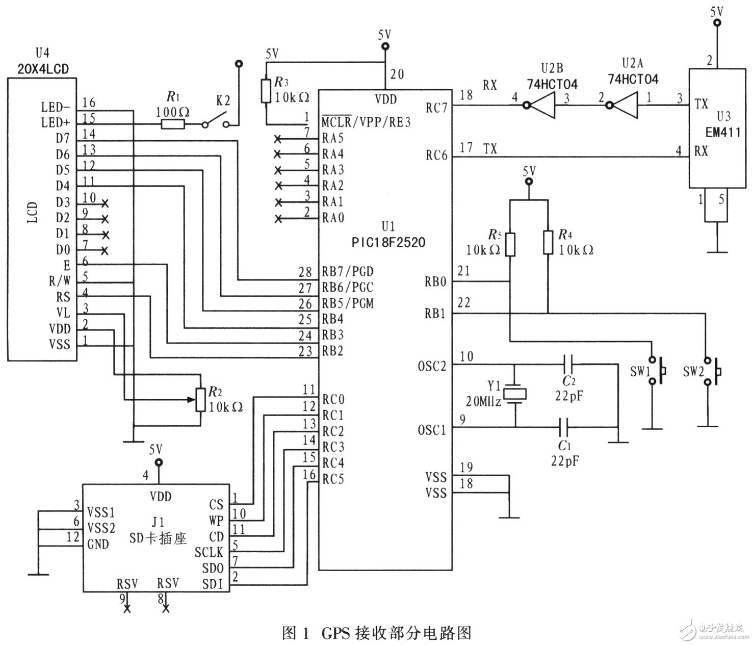
The system design uses a 20×4 dot matrix character liquid crystal display to display the received GPS positioning information. The liquid crystal display is set in 4 bit mode. The MCU saves MCUI/O by controlling the LCD display through 4 data lines and enable pins. Port resource. The system is equipped with 2 buttons for controlling the data storage of the SD card. When the SW1 button is pressed, the data save time interval is set by the software delay. When the SW2 button is pressed, the system writes the received GPS positioning information to the SD card. In Figure 1, switch K2 is used to turn the LCD backlight power on and off: the RA port resource of the PIC18F2520 is not used. It can be reserved for future system upgrades, such as inputting the DC analog voltage signal from the battery to the RA port and converting it to a digital signal using the PIC18F2520's 10-bit A/D converter. The battery level is displayed on the LCD for user convenience.
4.2 Power section
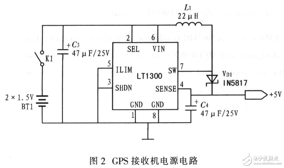
The portable GPS receiver is powered by two AA-size 1.5 V batteries and uses a micropower, high efficiency DC-DC converter LT1300 to convert 3 V to 5 V for use in the circuit. The LT1300 has a minimum input voltage as low as 1 .8 V, conversion efficiency up to 88%. With an input voltage of 2 V and an output voltage of 5 V, the LT1300's output current can reach 220 mA. The LT1300 is available in an 8-lead SOIC package with pin 1 signal ground (GND) and pin 2 output select (SEL). When connected to the input supply, it outputs 5 V. When this pin is grounded, the LT1300 Output 3.3 V voltage. Pin 3 (SHUTDOWN) is used to select the working mode. When this pin is grounded, the LT1300 is in normal operation mode; when this pin is connected to the high level, the LT1300 is in the power-down mode. Pin 4 (SENSE) is the output of the LT1300. Pin 5 is current limited. When this pin is grounded, its maximum switching current is 400 mA. Pins 6 to 8 of the LT1300 are the power input, output switch, and power ground. 2 is a GPS receiver power supply circuit composed of the LT1300. Switch K1 in Figure 2 is the total power switch of the GPS receiver. Since the main part of the GPS receiver uses 5 V, pin 2 and pin 6 of the LT1300 are connected to the positive terminal of the battery, and pin 3, pin 5, pin 1, and pin 8 are grounded. When working, pin 7 needs an external inductor and diode. Its function is that when the battery power consumption is too large, the switching effect inside the LT1300 will cause the current on the inductor L1 to alternately increase. At this time, the diode VD1 will dump this part of energy to Capacitor C4 to increase the output voltage of the LT1300. Refer to the recommended model and parameters in the LT1300 data sheet for the diodes designed in this section and the parameters of the inductor L1 and electrolytic capacitor C4. It should be noted that since the LT1300 is a high-speed, high-current device, the L1 should be placed close to the pin 7 as much as possible in the PCB layout. The trace should be as short as possible, and the power ground should be connected to the signal ground to reduce the circuit. Interference noise.
Geared Stepper Motor
Geared Stepper Motor,Planet Gearbox,Spur Gearbox,Nema23 Geared Electric Motor
Changzhou Sherry International Trading Co., Ltd. , https://www.sherry-motor.com