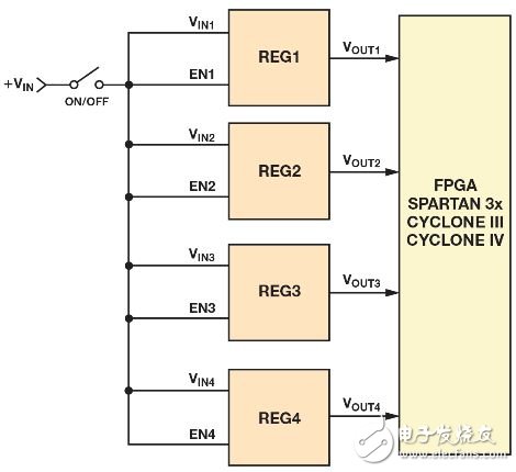
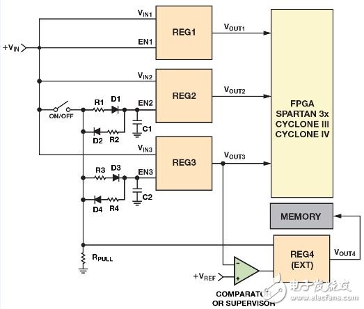
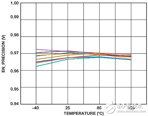
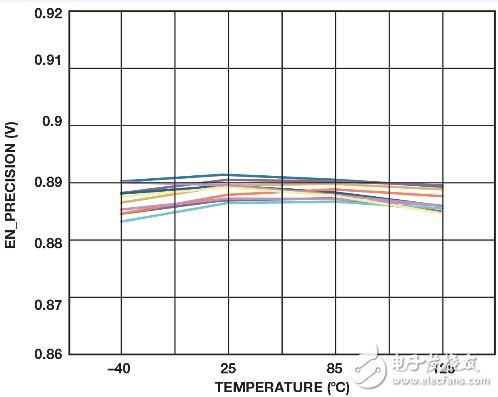
introduction This article discusses the advantages and disadvantages of using discrete devices for power sequencing. It also introduces a simple and effective way to implement timing control using the ADP5134's internal precision enable pins. The ADP5134 contains two 1.2-A buck regulators and two 300- mA LDO. At the same time, this article also lists a series of ICs that can be used in applications that require more precise and flexible timing control. Figure 1 shows an application that requires multiple power rails. These rails are core power (VCCINT), I/O power (VCCO), auxiliary power (VCCAUX), and system memory power. Figure 1. Typical power supply for processors and FPGAs For example, the Xilinx Spartan-3AFPGA has a built-in power-on reset circuit that allows the device to be configured after all power supplies have reached their thresholds. This helps reduce power supply timing control requirements, but to achieve minimum inrush current levels and follow the circuit timing control requirements for the FPGA, the power rail should power up VCC_INT → VCC_AUX → VCCO in the following sequence. Please note: Some applications require a specific sequence, so be sure to read the Power Requirements section of the data sheet. Simplify power sequencing with a passive delay network A simple way to achieve power sequencing is to use passive components such as resistors, capacitors, and diodes to delay the signal entering the regulator enable pin, as shown in Figure 2. When the switch is closed, D1 conducts and D2 remains open. Capacitor C1 is charged and the Voltage at EN2 rises at a rate determined by R1 and C1. When the switch is turned off, capacitor C1 is discharged to ground through R2, D2, and RPULL. The voltage at EN2 drops at a rate determined by R2, RPULL, and C2. Changing the values ​​of R1 and R2 will change the charge and discharge time, thus setting the regulator's on and off times. Figure 2. An easy way to implement power sequencing with resistors, capacitors, and diodes This method can be used for applications that do not require precision timing control, as well as for applications that require only delayed signals and may only require external R and C. A disadvantage of using this approach for standard regulators is that the logic threshold of the enable pin can vary greatly due to voltage and temperature. In addition, the delay in the voltage ramp depends on the resistance and capacitance values ​​and tolerances. Typical X5R capacitors vary by approximately ±15% over the –55°C to +85°C temperature range, with ±10% variation due to DC bias effects, making timing control inaccurate, sometimes It will also become unreliable. Precision enabling easy timing control In order to achieve a stable threshold level for precise timing control, most regulators require an external reference. The ADP5134 solves this problem by integrating a precision voltage reference, significant cost savings, and PCB area. Each regulator has a separate enable pin. When the enable input voltage rises above VIH_EN (minimum of 0.9 V), the device exits shutdown mode and the management module is turned on, but the regulator is not activated. Compare the voltage of the enable input to a precision internal reference voltage (typically 0.97 V). Once the voltage at the enable pin rises above the precision enable threshold, the regulator is activated and the output voltage begins to rise. At the input voltage and temperature transitions, the reference voltage varies by only ±3%. This small range of changes ensures precise timing control and solves a variety of problems with discrete devices. The regulator is deactivated when the voltage at the enable input drops below 80 mV (typical) below the reference voltage. The device enters shutdown mode when the voltage across all enable inputs drops below VIL_EN (maximum of 0.35 V). In this mode, the power consumption drops below 1 μA. Figures 3 and 4 show the accuracy of the ADP5134 precision enable threshold for Buck1 over temperature. Figure 3. Precision enable turn-on threshold in the temperature range (10 samples) Figure 4. Precision Enable Shutdown Threshold in Temperature Range (10 samples) 18650 2S6P 7.4V Battery Pack,Rechargeable Aa Batteries,Portable Battery Charger,External Battery Pack Ji'an Powercom New Energy Co., Ltd. , https://www.expowercome.com
Power sequencing is a must-have feature for microcontrollers, FPGAs, DSPs, ADCs, and other devices that require multiple rail rails. These applications typically require powering up the core and analog modules before the digital I/O rails are powered up, but some designs may require additional sequences. In any case, proper power-up and shutdown timing control can prevent immediate damage caused by latch-up and long-term damage caused by ESD. In addition, power sequencing can stagger the inrush current during power-up, a technique that is useful for applications that use current-limited power supplies.