ZOOKE provides solutions for pin to pin female connectors, policy connectors, round pin connectors, bent pin connectors, high current connectors, and line to board connectors. Pai Pin,Pai Mu,Pai Pin Pai Mu Zooke Connectors Co., Ltd. , https://www.zooke.com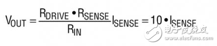
**Introduction**
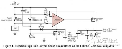
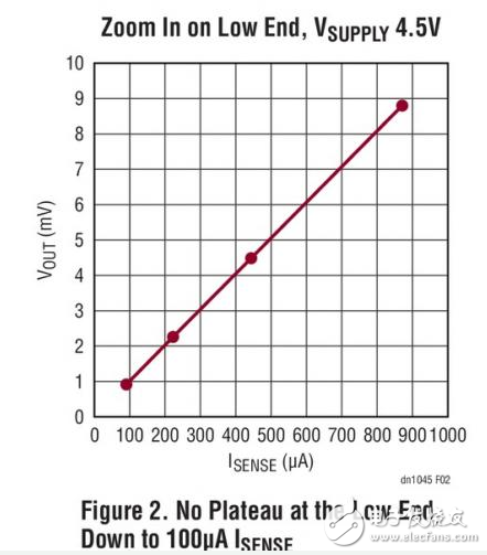
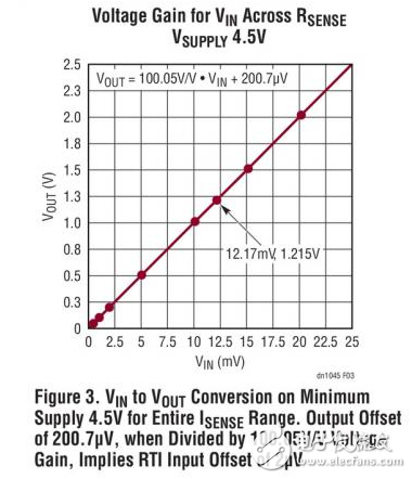
Accurate high-end measurement of microampere-level currents demands a small-value shunt resistor and an amplifier with low offset voltage and ultra-low power consumption. This design provides a 280μA supply current, allowing the circuit to sense currents ranging from 100μA to 250mA. This minimizes power loss across the shunt resistor while maximizing the available power for the load. The LTC2063’s rail-to-rail input allows operation at very low load currents, ensuring the input common-mode voltage remains within range. Additionally, its built-in EMI filter protects against RF interference in noisy environments. For a given sensed current, the output voltage is calculated using the formula: