Abstract: When using a high-frequency switching regulator, a good automotive power PCB layout can provide a cleaner output and simplify debugging in EMI testing. This article uses the MAX16903 / MAX16904 switching regulator design as an example to introduce how to route to obtain the best performance and reduce radiation.
introduction
When using a high-frequency switching regulator (such as the MAX16903 / MAX16904), a good automotive power PCB layout can provide a cleaner output and simplify the debugging work in electromagnetic interference (EMI) testing. This article takes the MAX16903 / MAX16904 switching regulator design as an example to introduce the layout principles for optimizing system performance.
General rules for wiring
Keep the loop area formed by the input capacitor C3, inductor L1, and output capacitor C2 to a minimum.
Place the BIAS output capacitor (C4) as close as possible to the 13th pin (BIAS) and 14th pin (GND), and avoid vias between the pin and the capacitor. This is the analog power input of the IC. Any inductance on the female wire will introduce noise in the BIAS power supply, thereby increasing the jitter of the LX output.
Use the shortest possible lead.
Optimize AC-DC current path
In order to reduce electromagnetic radiation as much as possible, the layout of the MAX16903 / MAX16904 peripheral components is critical. The path of the current jump is called the AC path and appears when the switch is ON / OFF. After the switch is turned on / off (ON / OFF), the current in the current path is the DC path.
AC path
The switching current path of the MAX16903 synchronous DC-DC converter requires three passive components (C2, C3, L1). These three components have a great influence on electromagnetic radiation and device performance. Figures 1 and 2 show the current paths during the ON and OFF periods; Figure 3 illustrates the difference between the two current paths with the highest di / dt. The wiring of C3 should be given priority, followed by the wiring of L1 and C2.
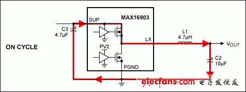
Figure 1. OUT2 current path with PMOS on
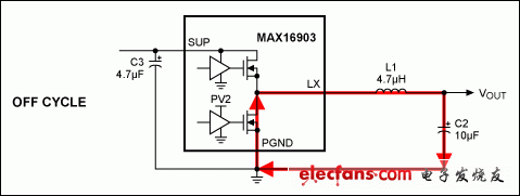
Figure 2. OUT2 current path with DMOS on
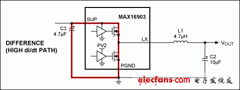
Figure 3. Differences in the AC path of OUT2
Vibratory Motor
Xinxiang Mina Import & Export Co., Ltd. , https://www.mina-motor.cn