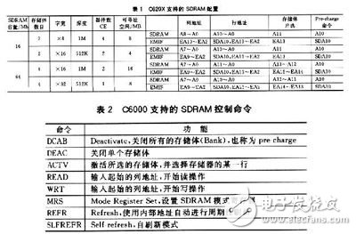
In high-speed signal processing applications such as digital image processing and aerospace, strong support for high-speed and large-capacity storage space is required to meet the system's requirements for massive data throughput. By using large-capacity synchronous dynamic RAM (SDRAM) to expand the storage space of the embedded DSP system, ISSI's IS42S16400 high-speed SDRAM chip is selected, and the specific design method of the digital signal processing system based on TMS320C6201 (referred to as C6201) is discussed in detail. achieve. 1 IS42S16400 chip introduction The IS42S16400 is a 16-bit word-wide high-speed SDRAM chip from ISSL that has a single-chip memory capacity of up to 64 Mb (8 MB). The main features of SDRAM are: 1 synchronous access, read and write operations require a clock; 2 dynamic storage, the chip needs to be refreshed periodically. The IS42S16400 uses a CMOS process. Its synchronous interface and fully pipelined internal structure allow it to have a very high data transfer rate. It can operate at clock frequencies up to 133 MHz with a refresh rate of 4096 cycles per 64 ms. The SDRAM chip has four banks inside, and the system address bus is time-multiplexed by row and column addresses to read and write access to specific memory cells of different pages in different memory banks. Before the read operation, the corresponding bank in the SDRAM must be activated in advance, and a certain row of the memory is selected, and then the column address is sent to read the required data. There is an access delay between the output column address and the corresponding data returned by the SDRAM. If you access a new page, you will need to close all the banks first, otherwise the opened page will remain valid. Prior to the write operation, since the relevant row address has been previously activated, the data can be output while the column address is being output without delay. The IS42S16400 provides self-refresh mode settings that allow the chip to operate in a low-power state, greatly reducing the power consumption of embedded systems. 2 C6201 and SDRAM external memory interface When the DSP chip accesses the off-chip memory, it must pass the external memory interface EM1F (External Memory Interface). The EMIF of the C6000 series of DSPs has a strong interface capability, which not only has high data throughput (up to 1200 MB/s), but also interfaces directly with almost all types of memory. In the C6201 system, four independent external memory interfaces (CEX) are provided. All external CEx spaces support direct interface to SDRAM, except that CEl space only supports asynchronous interfaces. Table 1 summarizes the EMIF-compatible SDRAM configurations for the C620XDSPs. Table 2 shows the SDRAM control commands supported by the EMIF of the C6000 series DSPs. 2.1 SDRAM refresh   To increase storage capacity, SDRAM uses silicon capacitors to store information. Over time, the capacitor must be recharged to maintain the data in the capacitor. This is called "refresh." Its existence also makes the application of SDRAM a little more complicated, which brings certain application difficulties. C6000 series DSPs have special SDRAM control registers (SDTCL) and SDRAM timing control registers (SDTIM), which are used to perform various timing control of SDRAM, which greatly reduces the development difficulty of designers. The RFEN bit in the SDCTL register controls whether the SDRAM is refreshed by the EMIF. If RFEN = 1, the EMIF controls the issue of a refresh command (REFR) to all SDRAM spaces; the PERIOD bit in the SDTIM register controls the specific refresh period. A DCAB command is automatically inserted before the REFR command to ensure that all SDRAMs are inactive during the refresh process. After the DCAB command, the EMIF begins timing refreshes according to the value set in the PERD field in the SDTIM register. The page information becomes invalid before and after the refresh. For the C620X, the EMIF SDRAM control module has a 2-bit counter inside to monitor the number of refresh requests submitted. The counter is incremented by one each time an application is submitted; the counter is decremented by one after each refresh cycle. On reset, the counter is automatically set to 11b to ensure several refreshes before accessing the access. The value of the counter is llb, which represents the emergency refresh state. At this time, the page information register becomes invalid, forcing the controller to close the current SDRAM page. Then, the EMIF SDRAM controller executes the REFR command three times after the DCAB command, reducing the value of the counter to 0, and then continuing to complete the remaining access operations. 2.2 SDRAM initialization When a CE space is configured as SDRAM space, it must be initialized first. The user does not need to control every step of the initialization. It only needs to write 1 to the INIT bit of the EMIF SDCTL register to request initialization of the SDRAM. Then, EMIF will automatically complete the steps required. The initialization operation cannot be performed during the SDRAM access process. The entire initialization process consists of the following steps: 1 issue a DCAB command to all SDRAM spaces; 2 execute 3 REFR commands; 3 Issue MRS commands for all SDRAM spaces. 2.3 page boundary control SDRAM is a paged memory. EMIF's SDRAM controller monitors the row address when accessing SDRAM, avoiding line crossings during access. To accomplish this task, the EMIF internally has four page registers that automatically save the currently open row address and then compare it with the address of subsequent accesses. It should be noted that the end of the current access operation does not cause the activated line in the SDRAM to be immediately turned off. The EMIF control principle is to maintain the current open state unless it must be closed. This has the advantage of reducing the command switching time between shutdown/reopening, allowing the interface to make full use of the address information during the control of memory access. For the C620X, each CE space contains 1 page register (only valid for SDRAM space configuration), so the C620X can only activate 1 page per CE space. The number of address bits to compare depends on the value of the SDWID bit in the SDCTL register. If SDWID=O, the size of the CE space composition page is 512, the logical address of the comparison is bits 23 to 11; if SDWID=1, the size of the CE space SDRAM page is 256, and the logical address of the comparison is bits 23 to 10. . Once the page is out of bounds, the EMIF automatically performs the DCAB operation and then starts a new row access. 2.4 Shift of the access address Since the SDRAM row logical address and the column logical address are multiplexed with the same EMIF pin, the EMIF interface needs to perform corresponding shift processing on the row address and the column address. The shift processing of the address is controlled by the SDW1D bit in the SDCRL register. In addition, for SDRAM, since the input address is also a control signal, the following points need to be explained: The upper address signal of the 1RAS active period is latched by the EMIF internal SDRAM controller to ensure that the correct bank is gated when the READ and WRT commands are executed; During 2READ/WRT operation, EMIF keeps the pre-charge signal low (C620X is SDAl0) to prevent auto pre-charge operation after the READ/WRT command is executed. 2.5 Interface timing design For the C620X, the interface timing of EMIF and SDRAM is controlled by the SDCTL register. The EMIF provides five timing parameters, three of which are set in the SDCTL register and the other two are fixed values, as listed in Table 3. When analyzing the fit of the interface timing, it is necessary to calculate the size of the "rich time" tmargin, which is a margin in the timing obtained after considering the worst case provided by the device manual of the SDRAM chip. As for the size of the tmargin value, it is a problem that the system design layer needs to consider. The specific requirements vary with different systems, and are closely related to the actual layout of the printed board and the load.       Â
The unique acicular radiator,360 degree dissipation small wind resistance. High heat dissipation efficiency ensuring that the LED chip can work for 50000 hours.
Color temperature 3000-6000K
Light≥90LM/W
Matching the 2.3.4 lane,tunnel and Landscape Lamp,floodlight dedicated lens.Ensure that intensity and uniformity.
Glare index Signification reduce the original LED Module size,removal of power supply problems.Low demands for application situation and installation personnel More suitable for the transformation of traditional lamps.
Technical parameters
Power :30W,30W,15W,15W
Structure size: 135×100×40 mm, 208×74×49 mm, 125×58×30mm, 380×40×25mm
Lens size: 135×100 mm, 186×64 mm, 125×58mm, 355×40mm
Input voltage: 220 V, 220 V ,220 V, 220 V
Input current: 0.132 A, 0.132 A ,0.123 A, 0.125 A
Luminous flux: 2760 LM ,2400 LM ,1230 LM ,1300 LM
Light effect: 92 LM/W 80 LM/W 82 LM/W 86 LM/W
Color temperature: 5000 K 5000 K 5000 K 5000 K
Power factor: 0.99 PF 0.98 PF 0.98 PF 0.99 PF
Working temperature: -40+50°C, -40+50°C, -40+50°C ,-40+50°C
Led Module,Led Modules For Signs,Led Module Bulb,Led Modules For Signage Jiangsu chengxu Electric Group Co., Ltd , https://www.satislighting.com