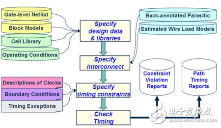
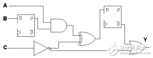
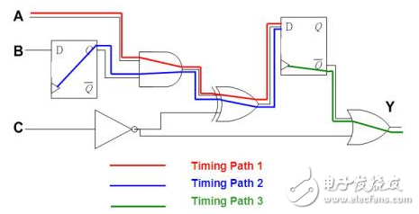
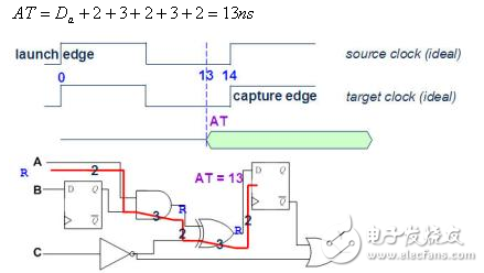
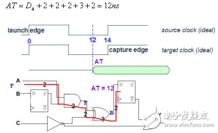
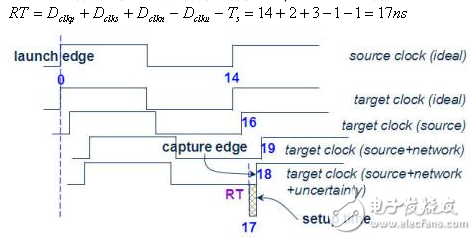
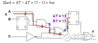
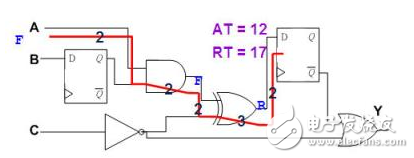
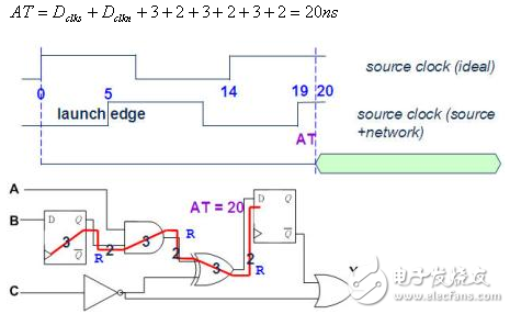
In addition to the Clock, the other output input terminals of the circuit and its surrounding environment (Boundary CondiTIon) are also described. Before explaining Boundary CondiTIon, we have to have a better understanding of the path. As mentioned above, STA will find out all the paths in the circuit for analysis, but what is the definition of Path? Path can be divided into four types according to the starting point and the ending point: Input from Flip-Flop Clock to Flip-Flop data input (top left of Figure 17). Figure XVII In general, we will define the following Boundary Condition: Driving Cell: Defines the driving ability of the input endpoint (Figure 18). Figure 18 Figure 19 Since each Path has a Timing Constraint, timing analysis can be performed. But in some cases, some Path analysis may not make sense, so you will want to ignore the analysis of these Paths. Or some Path analysis methods are different, you will want to specify the way these paths are analyzed. At this point, you should set some Timing Exceptions, such as False Path and Multi-cycle Path, to handle non-general timing analysis. STA process and analysis method The STA's process is shown in Figure 20, and its analysis and verification project is the Timing Arc related to the timing check mentioned in the previous article, such as Setup Time, Hold Time, and so on. Below we describe the STA's analysis method for the Setup Time. Figure twenty Setup Time The design circuit is shown in Figure 21. The Timing Model and Timing Constraint are as follows: Figure 21 The maximum delay time for all logic gates when the output signal rises is 3ns, and the shortest is 2ns. The maximum delay time for all logic gates when the output signal rises is 2ns, and the shortest is 1ns. The longest delay for all connections (Net) is 2ns and the shortest is 1ns. The delay time for all Flip-Flop Clocks to Q is 3ns. The setup time of all Flip-Flops is 1 ns (Ts). The Hold Time of all Flip-Flops is 1 ns (Th). The Clock period is 14ns (Dclkp). Clock source latency is 2ns (Dclks). Clock network latency is 3ns (Dclkn). The clock uncertainty is 1 ns (Dclku). The input delays of both B and C are 1 ns (Da, Db, Dc). The output delay of Y is 3ns (DY). Next, we explain the way of timing analysis in the form of Step-By-Step. 1. First find out all Timing Paths. We only list three representative Timing Paths to illustrate. Figure twenty two 2. Assuming that the input A signal changes from 0 to 1, calculate the time when the first Path end signal arrives (Arrival Time for short). Figure twenty three 3. Assuming that the input A signal changes from 1 to 0, the first Path end AT is calculated. Figure twenty four 4. Calculate the required time (RT) of the 1st Path end point. Figure twenty five 5. Assume that the input A signal changes from 0 to 1, and calculate the Slack at the end of the first Path. Slack is equal to the difference between RT and AT, equal to RT - AT for Setup Time verification, and equal to AT - RT for Hold Time verification. In this Setup Time example, Slack is positive, indicating that the signal actually arrives at the Path end time earlier than the time that must be reached, so Timing is satisfied. Figure twenty six 6. Assume that the input A signal changes from 1 to 0, and calculate the Slack at the end of the first Path. Slack is positive, so Timing is satisfied. Integral 5 and 6, the Timing of the first Path is in accordance with the specifications, and its Slack is 4 ns (poor condition). Figure twenty seven 7. Assume that the signal of the front-end Flip-Flop changes from 0 to 1, and calculates the AT of the second Path end.
What are the holes in a PCB called?
Generally, there are three types of PCB vias that we often see:
Buried Via Hole Pcb,Blind Via Hole Pcb,Multilayer Blind Buried Pcb Vias,Blind Via Pcb HAODA ELECTRONIC CO.,LIMITED , https://www.pcbhdi.com
From the primary input (PI) to the Flip-Flop data input (Figure 17 upper right).
Input from Flip-Flop Clock to Primary Output (PO) (bottom left in Figure 17).
From the main input to the main output (Figure 17 below right).
When the Clock specification is determined, the Timing Constraint of the first Path is automatically given. In order to give timing constraints for the other three paths, we must define Boundary CondiTIon. 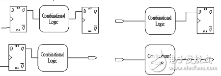
Input Transition Time: Defines the conversion time of the input endpoint (Figure 18).
Output Capacitance Load: Defines the output load (Figure 18).
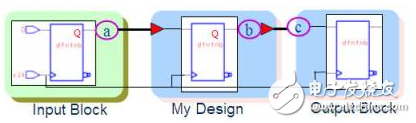
Input Delay: The delay time of the input endpoint relative to a certain Clock field. (Figure 19, Delayclk-Q + a)
Output Delay: The delay time relative to a certain Clock field from the output endpoint. (Figure 19, c)
After these Boundary Condition definitions, the above four paths can actually be regarded as the first Path (Flip-Flop to Flip-Flop). That is to say, after adding the Boundary Condition, as long as the Clock is given, Timing Constraint of all Paths will be given automatically. 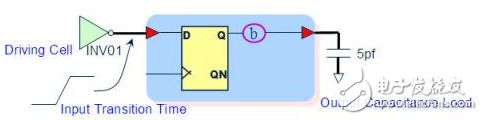
Through Hole: Plating Through Hole abbreviated as PTH, this is the most common one, you only need to pick up the PCB and face the light, the hole that can see the bright light is the "through hole". This is also the simplest type of hole, because when making it, you only need to use a drill or a laser to directly drill the circuit board, and the cost is relatively cheap. But on the other hand, some circuit layers do not need to connect these through holes. For example, we have a six-story house. I bought its third and fourth floors. I want to design a staircase inside that only connects the third floor to the third floor. It's fine between the fourth floor. For me, the space on the fourth floor is invisibly used up by the original staircase connecting the first floor to the sixth floor. So although through holes are cheap, they sometimes use up more PCB space.


